Method for plasma stripping using periodic modulation of gas chemistry and hydrocarbon addition

a technology applied in the field of plasma stripping using periodic modulation of gas chemistry and hydrocarbon addition, can solve the problems of cd enlargement, pattern distortion, striation, etc., and achieve the effect of decreasing increasing the thickness of the protective layer

Inactive Publication Date: 2007-11-13
LAM RES CORP
View PDF54 Cites 29 Cited by
  • Summary
  • Abstract
  • Description
  • Claims
  • Application Information

AI Technical Summary

Benefits of technology

[0007]To achieve the foregoing and in accordance with the purpose of the present invention, a method for etching a feature in a low-k dielectric layer through a photoresist etch mask over a substrate is provided. A low-k dielectric layer is placed over a substrate. A patterned photoresist mask is placed over the low-k dielectric layer. At least one feature is etched into the low-k dielectric layer. A gas-modulated cyclic stripping process is performed for more than three cycles for stripping a single photoresist mask. Each cycle of the gas-modulated cyclic stripping process comprises performing a protective layer formation phase and a stripping phase. The protective layer forming phase using first gas chemistry with a deposition gas chemistry, wherein the protective layer forming phase is performed in about 0.005 to 10 seconds for each cycle, comprises providing the first gas chemistry and forming a plasma from the first gas chemistry, wherein a protective layer is formed on sidewalls of the at least one feature and a thickness of the protective layer is increased. The performing the stripping phase for stripping the photoresist mask using a second gas chemistry using a stripping gas chemistry, where the first gas chemistry is different than the second gas chemistry, wherein the etching phase is performed in about 0.005 to 10 seconds for each cycle comprises providing the second gas chemistry and forming a plasma from the second gas chemistry, wherein the thickness of the protective layer is decreased and some of the photoresist mask is stripped.

Problems solved by technology

During the etching process, the mask materials are usually eroded and / or damaged in exchange for the pattern transfer.
Consequently, some of the damage and erosion also may be transferred to the underlying layers leaving such undesirable pattern distortions such as striation, CD enlargement, faceting, etc.
In addition, for low-k dielectric materials (k<3.0), during the stripping of the photoresist, damage may occur to the low-k dielectric material, which may increase the k value.

Method used


Image

  • Method for plasma stripping using periodic modulation of gas chemistry and hydrocarbon addition
  • Method for plasma stripping using periodic modulation of gas chemistry and hydrocarbon addition
  • Method for plasma stripping using periodic modulation of gas chemistry and hydrocarbon addition

Examples


example

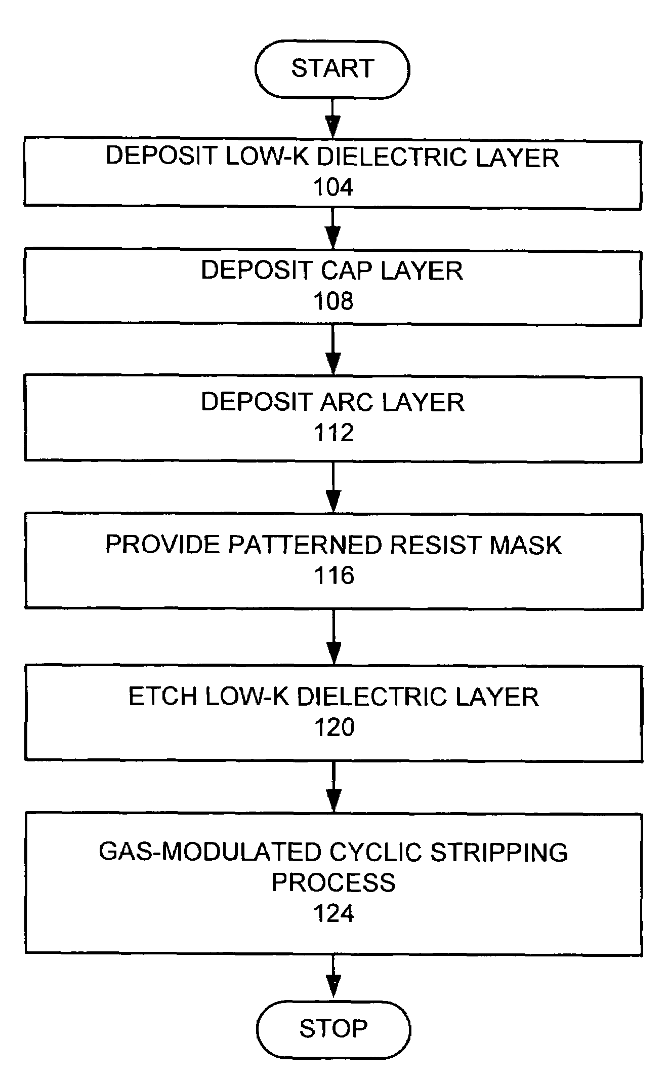
[0091]In an example of the invention, a low-k dielectric layer of OSG was placed over a substrate (step 104). A silicon oxide cap layer was deposited over the low-k dielectric layer (step 108). The cap layer is about 500 Å thick. An organic ARC layer was formed over the cap layer (step 112). A patterned photoresist mask was formed over the ARC (step 116). In this example, the photoresist was 193 nm PR from Shipley.

[0092]The substrate was then placed in a process chamber. FIG. 5 is a schematic view of a process chamber 500 that may be used in the preferred embodiment of the invention. In this embodiment, the plasma processing chamber 500 comprises confinement rings 502, an upper electrode 504, a lower electrode 508, a gas source 510, and an exhaust pump 520. Within plasma processing chamber 500, the substrate wafer 580, over which the oxide layer is deposited, is positioned upon the lower electrode 508. The lower electrode 508 incorporates a suitable substrate chucking mechanism (e.g...


PUM

PropertyMeasurementUnit
thickaaaaaaaaaa
total cycle timeaaaaaaaaaa
cycle timeaaaaaaaaaa

Abstract

A method for etching a feature in a low-k dielectric layer through a photoresist etch mask over a substrate. A gas-modulated cyclic stripping process is performed for more than three cycles for stripping a single photoresist mask. Each cycle of the gas-modulated cyclic stripping process comprises performing a protective layer formation phase and a stripping phase. The protective layer forming phase using first gas chemistry with a deposition gas chemistry, wherein the protective layer forming phase is performed in about 0.005 to 10 seconds for each cycle. The performing the stripping phase for stripping the photoresist mask using a second gas chemistry using a stripping gas chemistry, where the first gas chemistry is different than the second gas chemistry, wherein the etching phase is performed in about 0.005 to 10 seconds for each cycle.

Description

RELATED APPLICATIONS[0001]This application is a continuation-in-part of U.S. patent application Ser. No. 10 / 411,520, now U.S. Pat. No. 6,916,746, entitled “METHOD FOR PLASMA ETCHING USING PERIODIC MODULATION OF GAS CHEMISTRY,” by Hudson et al. filed Apr. 9, 2003, which is hereby incorporated by reference.BACKGROUND OF THE INVENTION[0002]1. Field of the Invention[0003]The invention relates to a method of obtaining a structure on a semiconductor wafer by etching through structures defined by a photoresist mask and then stripping the mask.[0004]2. Description of the Related Art[0005]In semiconductor plasma etching applications, a plasma etcher is usually used to transfer a mask pattern into a circuit and line pattern of a desired thin film and / or filmstack (conductors or dielectric insulators) on a wafer. This is achieved by etching away the films (and filmstacks) underneath the photoresist materials in the opened areas of the mask pattern. This etching reaction may be initiated by the...

Claims


Application Information

Patent Timeline
Patent Type & Authority Patents(United States)
IPC IPC(8): H01L21/00G03F7/42H01L21/302H01L21/3065H01L21/311H01L21/461
CPCH01L21/31116H01L21/76829H01L21/76802H01L21/31138H01L21/3065H01L21/306H01L21/311
Inventor YUN, SEOKMINZHU, JICIRIGLIANO, PETERLEE, SANGHEONCHOI, THOMAS S.LOEWENHARDT, PETERWILCOXSON, MARK H.SADJADI, REZAHUDSON, ERIC A.TIETZ, JAMES V.
Owner LAM RES CORP
Why Eureka
Try Eureka