Display panel, electrode panel and electrode substrate thereof

a technology of electrode substrate and substrate, which is applied in the direction of discharge tube luminescnet screen, instruments, natural mineral layered products, etc., can solve the problems of reducing the adhesion and pinhole formation reducing the adhesion of thicker metal thin films, and reducing the adhesion. , to prevent the conductive lines from being oxidized or even burnt out, the effect of enhancing the adhesion

Inactive Publication Date: 2007-11-13
RITDISPLAY
View PDF8 Cites 0 Cited by
  • Summary
  • Abstract
  • Description
  • Claims
  • Application Information

AI Technical Summary

Benefits of technology

[0018]As mentioned above, the display panel of this invention and its electrode substrate and electrode panel has two barrier layers for protecting the conductive layer (conductive lines). Compared to the prior art, this invention possesses the following advantages. Firstly, the barrier layers of the invention can prevent the conductive layer from being oxidized owing to the exposure of the UV light, and thus prevent increasing the resistance of the conductive layer and enhance the adhesion between the conductive layer and the photoresist layer. Meanwhile, when the display panel works, the barrier layers also may prevent the conductive lines from the influence of the external oxygen or sulfur, and thus prevent the conductive lines from being oxidized or even burnt out. Secondly, the adhesions between the conductive lines and the driving device and between the conductive lines and the electrode layer can be improved owing to the barrier layers of the invention, which may further ensure the reliability of the display panel. Thirdly, the invention may further control the shape of the patterned conductive line. For example, regarding to the shape of the cross-section of the conductive line, the middle portion of the conductive line is narrower than the side portions close to the first barrier layer and the second barrier layer, wherein the shape looks like a sandglass. Thus, the adhesion area between the conductive line and the electrode layer and the adhesion area between the conductive line and the driving device are larger than those of the prior art. That is, if the area of the electrode substrate is fixed, the adhesion area between the conductive line and the electrode layer of the invention is larger than that of the prior art. Hence, the adhesions therebetween are more reinforced, so as to ensure the reliability of the display panel. Fourthly, this invention may be implemented using one etchant. Therefore only one etching step is required to simultaneously etch the three-layer structure of the barrier layers and the conductive layer. Fifthly, since this invention is quite suitable in the practical industry because this invention has simple manufacturing processes and the overall cost is not significantly increased.

Problems solved by technology

However, the thinner metal conductive lines may increase the resistance of the conductive lines, resulting in that the RC-delay of signals is enlarged.
Therefore, the size of the flat panel display composing of the transition metals is restricted.
The thicker metal thin film, however, has the drawbacks of worse adhesion and pinhole formation.
In the current moment, although a special taper etching process is used to improve the drawbacks, the manufacturing cost is increased accordingly.
Moreover, the wider metal thin film not only decreases the aspect ratio of the pixels, but also increases the parasitic capacitance of the conductive lines.
Thus, the thicker and wider metal conductive lines can not be applied to flat panel display.
However, the planarization process needs additional processing steps and materials, and the result of the planarization may further increase the parasitic capacitance.
This may result in the reliability problem of the flat panel display.
However, copper is bad adhering to the glass substrate, the surface of copper is easy to be oxidized, and copper is hard to be etched away.
Therefore, the change of the manufacturing process or the composition is inevitable, which results in the increase of the manufacturing cost and complexity.
This is not matching the requirement for mass production of organic electroluminescent device.
Thus, three times of etching processes are necessary, resulting in complex manufacturing processes and increasing the cost.
In practice, the three-layer structure is unsuitable for the industrial application.

Method used


Image

  • Display panel, electrode panel and electrode substrate thereof
  • Display panel, electrode panel and electrode substrate thereof
  • Display panel, electrode panel and electrode substrate thereof

Examples


first embodiment

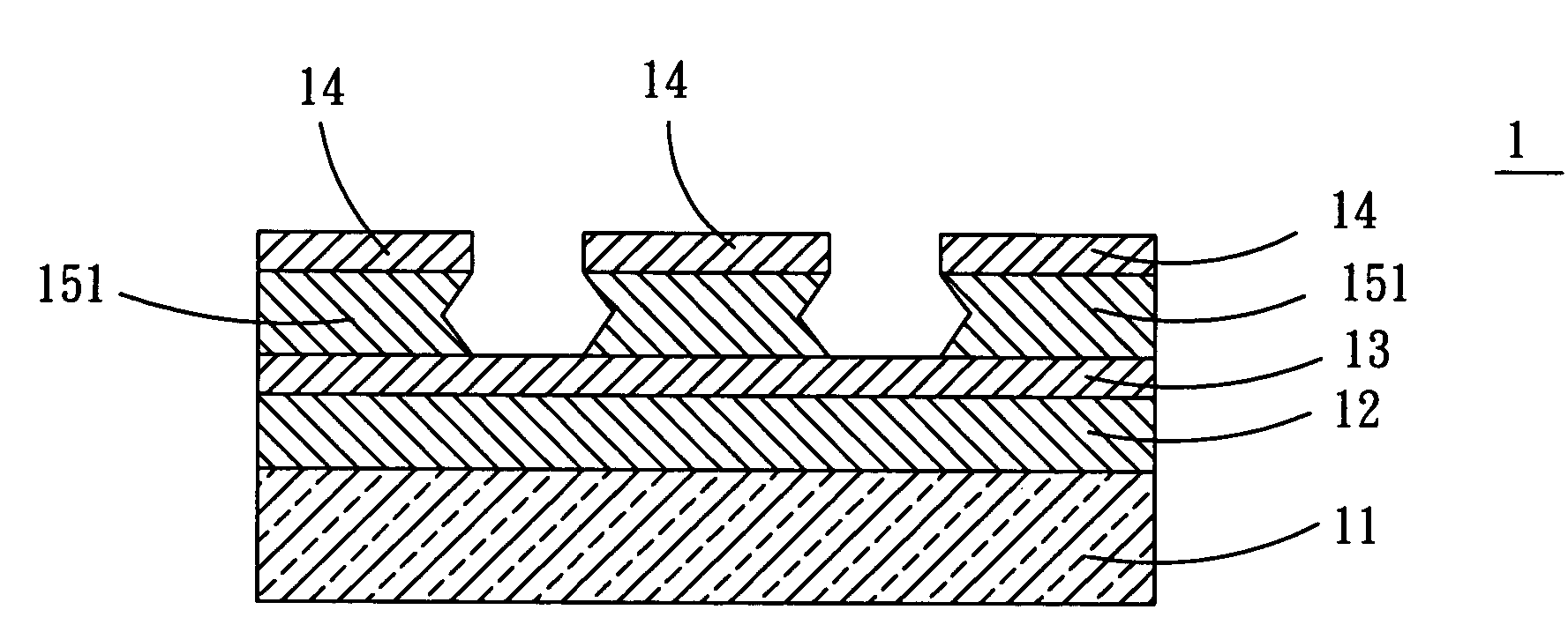
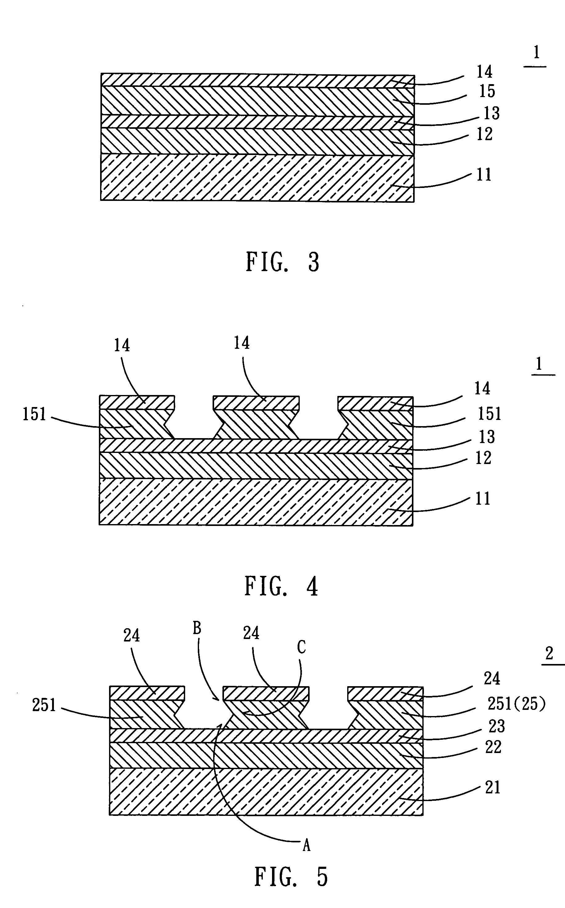
[0029]Referring to FIG. 3, an electrode substrate 1 of a flat panel display according to the invention comprises a substrate 11, an electrode layer 12, a first barrier layer 13, a second barrier layer 14, and a conductive layer 15. The electrode layer 12 is disposed on the substrate 11, the first barrier layer 13 is disposed on the electrode layer 12, the second barrier layer 14 is disposed above the first barrier layer 13, and the conductive layer 15 is disposed between the first barrier layer 13 and the second barrier layer 14.

[0030]In the present embodiment, the substrate 11 can be a flexible or a rigid substrate. The substrate 11 can also be a plastic or glass substrate. In particular, the flexible substrate or plastic substrate can be made of polycarbonate (PC), polyester (PET), cyclic olefin copolymer (COC), or metallocene-based cyclic olefin copolymer (mCOC).

[0031]Referring to FIG. 3, the electrode layer 12 is disposed on the substrate 11. In this embodiment, the electrode la...

second embodiment

[0042]Referring to FIG. 5, an electrode panel 2 of a flat panel display according to the invention comprises a substrate 21, an electrode layer pattern 22, a first barrier layer pattern 23, a second barrier layer pattern 24, and a conductive line pattern 25. In this embodiment, the electrode layer pattern 22 is disposed on the substrate 21 and has a plurality of electrode lines 221. The first barrier layer pattern 23 is disposed on the electrode layer pattern 22, and the second barrier layer pattern 24 is disposed above the first barrier layer pattern 23. The conductive line pattern 25 is disposed between the first barrier layer pattern 23 and the second barrier layer pattern 24. The conductive line pattern 25 has at least one conductive line 231.

[0043]In this embodiment, the electrode lines 221 of the electrode layer pattern 22 are parallel with each other or one another.

[0044]The features and functions of the substrate 21, the electrode layer pattern 22, and the barrier layer patt...

third embodiment

[0048]Referring to FIGS. 6A and 6B, a display panel 3 of a flat panel display according to the invention comprises a substrate 31, a light-emitting region 32, a driving device 33, a first barrier layer 34, a second barrier layer 35, and a conductive line pattern 36. The light-emitting region 32 has a plurality of pixels, and each of the pixels has a first electrode 321, a second electrode 323 and a light-emitting layer 322. The first electrode 321 is disposed on the substrate 31. The second electrode 323 is disposed above the first electrode 321. The light-emitting layer 322 is disposed between the first electrode 321 and the second electrode 323. The driving device 33 drives the pixels. The first barrier layer 34 is disposed above the substrate 31. The second barrier layer 35 is disposed above the first barrier layer 34. The conductive line pattern 36 is disposed between the first barrier layer 34 and the second barrier layer 35. The conductive line pattern 36 has a plurality of co...


PUM

PropertyMeasurementUnit
voltageaaaaaaaaaa
conductiveaaaaaaaaaa
flexibleaaaaaaaaaa

Abstract

An electrode substrate of a flat panel display at least comprises a substrate, an electrode layer, a first barrier layer, a second barrier layer and a conductive layer. The electrode layer is disposed above the substrate. The first barrier layer is disposed above the electrode layer. The second barrier layer is disposed above the first barrier layer. The conductive layer is disposed between the first barrier layer and the second barrier layer.

Description

BACKGROUND OF THE INVENTION[0001]This Non-provisional application claims priority under 35 U.S.C. § 119(a) on Patent Application No(s). 092117862 filed in Taiwan on Jun. 30, 2003, the entire contents of which are hereby incorporated by reference.[0002]1. Field of Invention[0003]The invention relates to a display panel, an electrode substrate and an electrode panel thereof and, in particular, to a display panel of a flat panel display, an electrode substrate of a flat panel display, and an electrode panel of a flat panel display.[0004]2. Related Art[0005]Referring to FIG. 1, the currently used electrode substrate 4 of a flat panel display includes a substrate 41, an electrode layer 42, and a conductive layer 43. The electrode layer 42 is disposed on the substrate 41, and the conductive layer 43 is disposed on the electrode layer 42. The material of the conductive layer 43 is selected from low resistance metals or the alloys thereof, such as a commonly used chromium or silver alloy.[0...

Claims


Application Information

Patent Timeline
Patent Type & Authority Patents(United States)
IPC IPC(8): H01J1/62B32B9/00H01J63/04G02F1/1345G09G3/00H01J1/02H01L27/32H05B33/00H05B44/00
CPCG02F1/1345H01J1/02H01L27/329H01L51/5212H01L27/3279Y10S428/917H10K59/1795H10K59/1315H10K50/814
Inventor WU, CHAO CHINLIAO, MENG-CHIEHLEE, JIUN-HAW
Owner RITDISPLAY
Why Eureka
Try Eureka