Electro-optical circuit board

a technology of optical circuit board and electro-optical circuit board, which is applied in the direction of circuit optical details, optical elements, instruments, etc., can solve the problems of affecting the transmission distance, the attenuation and distortion of signals, and the difficulty of the ic to achieve a high frequency connection to the external device, so as to avoid the deformation or damage of the optical waveguide, the effect of increasing the stiffness of the whole electro-optical circuit board and high pressure

Active Publication Date: 2007-11-13
IND TECH RES INST
View PDF5 Cites 9 Cited by
  • Summary
  • Abstract
  • Description
  • Claims
  • Application Information

AI Technical Summary

Benefits of technology

[0015]In the present invention, the following functions are achieved. 1. The optical waveguide is combined with the process for manufacturing PCB, and the optical waveguide becomes a layer in the PCB, so as to transmit the optical signal. 2. Copper is used to fabricate the optical guiding layer, and the stiffness of the whole electro-optical circuit board is increased, so as to avoid the deformation or damage of the optical waveguide due to the high temperature and the high pressure effect in the laminating process. 3. After the optical guiding layer made of copper is properly processed or coated, a preferred reflecting surface is formed to increase the optical coupling efficiency, and to reduce the transmitting loss of the common optical waveguide and the optical interference between multi-channel optical waveguides. 4. It is compatible with the conventional laminating process, and it is not necessary to particularly develop the laminating flow or table in order to develop the electro-optical circuit board technology, so the fabricating cost of the electro-optical circuit board is greatly reduced.

Problems solved by technology

The forecasting of the International Technology Roadmap for Semiconductor (ITRS) shows that, the frequency of the microprocessor reaches up to 10 GHz in 2011, but it is not easy for the IC to achieve a high frequency connection to the external device.
Nowadays, the electrically interconnection of the chip is constructed on the printed circuit board (PCB), on the electrical switching joint, via holes, and branches, and the discontinuous impedance causes the attenuation and the distortion of the signal, and even worse, the transmitting distance is influenced.
The conventional electrical connecting performance is greatly limited by the signal attenuation, the electromagnetic radiation and interference.
The optical waveguide is fabricated by the polymer material, and it is easily deformed in the high temperature and the high pressure, and the transition temperature of the optical waveguide is only about 180° C. In the laminating process with high temperature and high pressure, the optical path of the whole optical waveguide is offset, and even if it returns to the normal temperature and normal pressure, it is impossible to return to the expected optical coupling efficiency, so as to result in the great loss of the optical signal.

Method used


Image

  • Electro-optical circuit board
  • Electro-optical circuit board
  • Electro-optical circuit board

Examples


Embodiment Construction

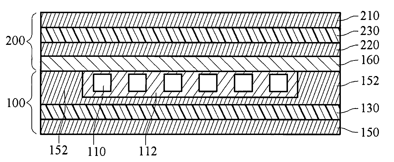
[0025]Referring to FIG. 4, it is a schematic view of an optical wiring board 100 of an electro-optical circuit board according to a first embodiment of the present invention. As shown in FIG. 4, the optical wiring board 100 of the first embodiment of the present invention includes a metal substrate 150, a glass fiber layer 130 formed on the metal substrate 150, an optical guiding layer 120 formed on the glass fiber layer 1301 and a metal supporting structure 152 formed around the optical guiding layer 120 and on the glass fiber layer 130.

[0026]The optical guiding layer 120 is formed by an optical waveguide and a clad 112. In this embodiment, the optical waveguide is a multi-channel optical waveguide, which includes a plurality of cores 110 embedded in the clad 112, such that the clad 112 totally wraps the cores 110. Since the index of refraction of the material of the clad 112 is smaller than that of the cores 110, when transmitting the optical signal, the optical signal is only tra...


PUM

PropertyMeasurementUnit
frequencyaaaaaaaaaa
angleaaaaaaaaaa
transition temperatureaaaaaaaaaa

Abstract

An electro-optical circuit board is provided, which includes an electrical wiring board and an optical wiring board. The optical wiring board includes a first metal substrate, an optical guiding layer formed on the first metal substrate, and a metal supporting structure formed around the optical guiding layer, wherein the optical guiding layer includes an optical waveguide and a clad wrapping the optical waveguide. When the electrical wiring board is joined with the optical wiring board through a laminating process, the metal supporting structure absorbs the pressure applied to the electro-optical circuit board.

Description

CROSS-REFERENCE TO RELATED APPLICATIONS[0001]This non-provisional application claims priority under 35 U.S.C. § 119(a) on Patent Application No(s). 095139346 filed in Taiwan, R.O.C. on Oct. 25, 2006, the entire contents of which are hereby incorporated by reference.BACKGROUND OF THE INVENTION[0002]1. Field of Invention[0003]The present invention relates to an electro-optical circuit board, and more particularly, to an electro-optical circuit board having an optical waveguide supporting structure.[0004]2. Related Art[0005]With the development of Internet, people's demanding on the bandwidth of the network is increasingly high, and the optical network has gradually developed towards the trend of large volume, variable changes, high reliability, and cost efficiency. The optical communication has been developed from the backbone network, the metropolitan network, the access network, the storing network towards completely achieving the optical fiber, and furthermore, the optical networki...

Claims


Application Information

Patent Timeline
Patent Type & Authority Patents(United States)
IPC IPC(8): G02B6/12G02B6/10G02B6/26G02B6/42G02F1/035G02F1/295
CPCG02B6/12G02B6/13H05K1/0274G02B6/4214H05K2203/061H05K3/4641
Inventor WU, CHERNG-SHIUNCHIU, HSIEN-HUANLEE, SHIN-GECHEN, YING-CHIH
Owner IND TECH RES INST
Why Eureka
Try Eureka