
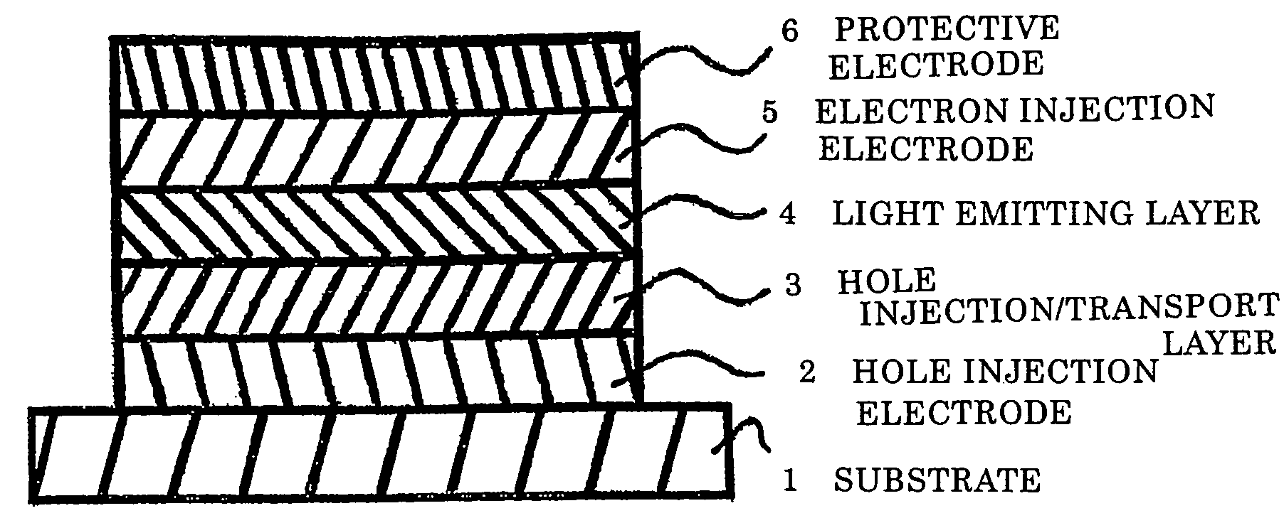
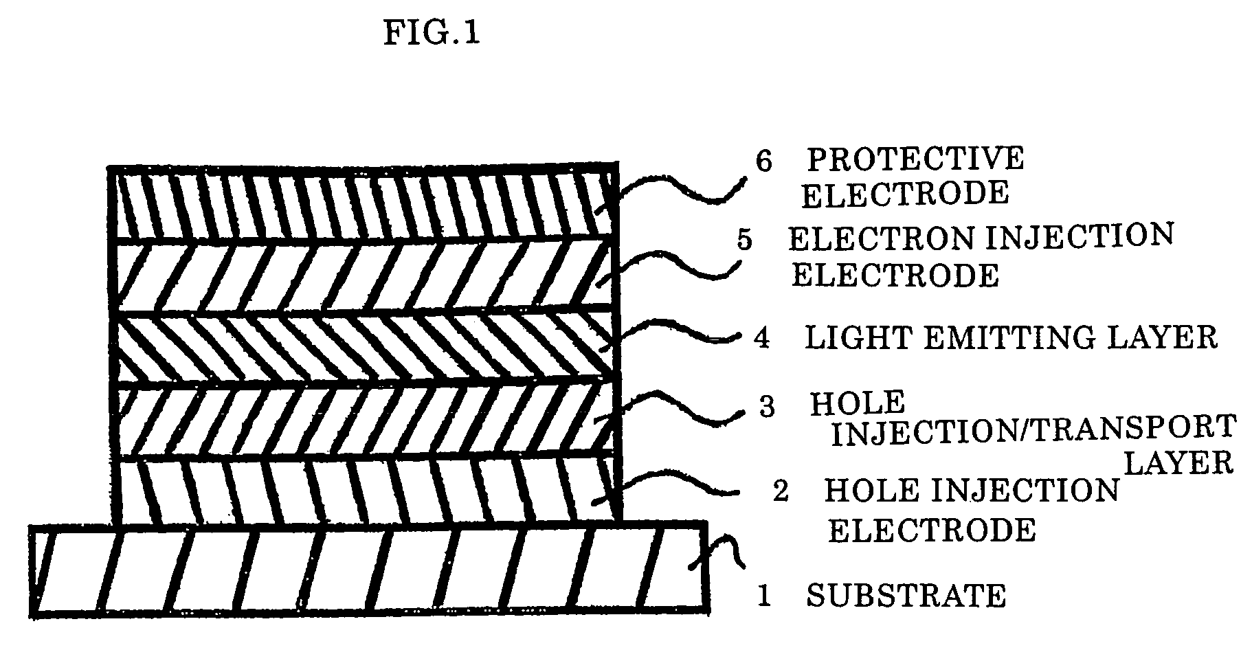
El device

a technology of electrodes and electrodes, which is applied in the field of electrodes for use in el devices, can solve the problems of insufficient improvement of electrodes described in any of the above-described publications, and achieve the effects of stable electrode efficiency, low resistance, and rapid enhancement of device li

Inactive Publication Date: 2007-12-18
NIPPON SODA CO LTD
View PDF9 Cites 14 Cited by
  • Summary
  • Abstract
  • Description
  • Claims
  • Application Information

AI Technical Summary

Benefits of technology

The present invention provides an electroluminescent device (EL device) that can be driven at a low voltage or current and has a high luminance as compared to conventional electrodes. The invention solves problems associated with conventional electrodes by setting specific values for the orientation of the crystal, size of the crystal, flatness of the film surface, and atomic composition of the film. The invention also provides a method for manufacturing a conductive film for use in the EL device. The technical effects of the invention include improved interface stability between layers in the device, reduced influence on organic compounds in the light emitting layer, and reduced surface roughness of the electrodes.

Problems solved by technology

There has been a problem that the improvement of the electrode described in any of the above-described publications is insufficient as an improvement for obtaining an EL device driven at a lower voltage to emit a light with a high luminance.

Method used


Image

  • El device
  • El device

Examples


example 1

[0135]An ITO film was prepared on a glass substrate by a pyro-sol method. That is, an alkali glass substrate (250×250×1 mm) pre-coated with an SiO2 film (film thickness of 150 nm) was projected into a conveyor furnace heated at 500° C. by a belt conveyor, an acetyl acetone solution of stannic chloride-indium acetyl acetone containing 5% by atom of tin atoms was formed in fog drips. Air was used as a carrier gas, blown into the conveyor furnace, brought into contact with the surface of a glass substrate, and thermally decomposed to form the ITO film. A surface resistance value of the obtained ITO film was 25 Ω / □ and a film thickness was 100 nm. In observation of the film surface by AFM, 100 or more 5 nm to 30 nm protrusions were observed in a 1 μm square, an average surface roughness (Ra) was 1.5 nm, and a maximum surface roughness (Rmax) was 18 nm. As a result of X-ray diffraction, the film was preferentially oriented in a (400) surface, and an X-ray intensity ratio of (400) / (222) w...


PUM

PropertyMeasurementUnit
sizeaaaaaaaaaa
surface roughnessaaaaaaaaaa

Abstract

The present invention relates to an EL device which is driven with a lower voltage or power amount, which is superior in interface stability between layers in the device and which has a higher luminance as compared with the use of a conventional electrode, and is characterized in that in the EL device comprising a light emitting layer disposed as an essential layer between two electrodes facing each other, at least one of the electrodes includes a crystalline conductive film whose diffraction intensity ratio of (400) / (222) is 1.0 or more in X-ray diffraction by a θ / 2θ method.

Description

TECHNICAL FIELD[0001]The present invention relates to an electrode for use in an EL device, further particularly to an improvement of a hole injection electrode which supplies a hole (positive hole) to a light emitting layer using an organic compound.BACKGROUND ART[0002]In recent years, considerable research has been done on an organic EL device. It has been noted that this is a device having a basic constitution in which hole transport materials such as triphenyl diamine (TPD) are formed into a thin film on a hole injection electrode by vapor deposition, fluorescent materials such as alumiquinolinol complex (Alq3) are further stacked as a light emitting layer, and metal electrodes (electron injection electrode) having a small work function, such as Mg, are formed, and a remarkably high luminance of several 100 to several 10,000 cd / m2 is obtained at a voltage of around 10 V.[0003]It is considered that materials for use as the hole injection electrode of the organic EL device, which ...

Claims


Application Information

Patent Timeline
Patent Type & Authority Patents(United States)
IPC IPC(8): H01L51/50H10K99/00
CPCH01L51/5206H01L51/0096Y10T428/24355Y10S428/917H01L51/5221H10K77/10H10K50/81H10K2101/00H10K59/8052H10K59/8051H05B33/26H10K50/82
Inventor SUZUKIGONDAIRA, HIDEAKITANIGUCHI, YOSHIO
Owner NIPPON SODA CO LTD
Learn More