Electrostatic chuck

a technology of electrostatic chuck and chuck body, which is applied in the direction of electrostatic holding device, basic electric elements, electric apparatus, etc., can solve the problems of heat resistance properties, requiring smoothness and lack of pinhole, and insulating film b>52/b> might be broken, etc., to prevent insulation breakdown, excellent characteristics of releasing the wafer w, excellent durability against plasma

Inactive Publication Date: 2007-12-25
KYOCERA CORP
View PDF13 Cites 22 Cited by
  • Summary
  • Abstract
  • Description
  • Claims
  • Application Information

AI Technical Summary

Benefits of technology

[0023]It an object of the present invention to provide an electrostatic chuck which can prevent an insulating film from cracking and breakdown of insulation with an excellent release characteristics of wafer.
[0033]According to the above constitution, no cracking occurs in the insulating film and the insulation breakdown can be prevented. Furthermore, the electrostatic chuck with an excellent characteristics of releasing the wafer W can be obtained.
[0034]Moreover, formation of a protective film can provide the electrostatic chuck with an excellent durability against plasma.

Problems solved by technology

But if it is too much, insulation of the insulating film 52 might be broke down.
Therefore, the surface of the insulating film 52 for holding an object requires smoothness and lack of pinhole.
However, these insulating film have problems in view of heat resisting properties, wear resistance, chemical resistance, etc., as well as cleanliness because abrasive powder which is generated in operation is likely to stick to a semiconductor wafer with bad influence.
This insulating film has a number of pinholes with a problem of withstand voltage.
But these have a problem of cracking due to the difference of the thermal expansion between the aluminum base and the insulating film when temperature is rising.
The insulating film in the electrostatic chuck disclosed in the documents 3 and 5 is formed using sputtering or CVD, the thickness of which is limited to a few micrometers or less, therefore, causing a possibility that the insulation of the insulating film is broken down when voltage is applied to the chucking electrodes.
But in such a protective film with a thickness of about 10 μm, pinholes which are created at a film forming step cannot be filled in, thereby eroding the underlayer.
In addition, such a film with a thickness of 0.1 to 10 μm is easily eroded under a hard plasma condition, so lacking for practicality.
This film also has a problem of flaking off due to an internal stress when forming the film having a thickness of 10 μm or more.
Thus these response of chucking and release characteristics is degraded and it takes excessive time to attach or detach the wafer, resulting in disadvantage for the process control.
But the sealed portion of silicon is easy to be etched by plasma, thereby lowering the withstand voltage.

Method used


Image

  • Electrostatic chuck
  • Electrostatic chuck
  • Electrostatic chuck

Examples


example 1

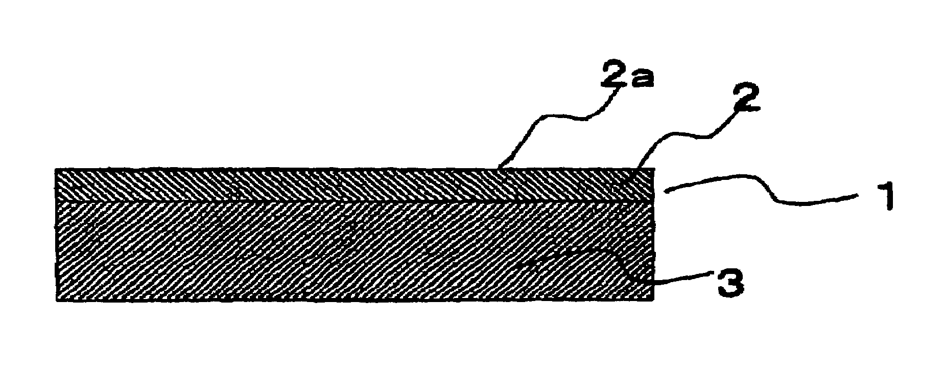
[0086]A porous body of SiC with a diameter of 198 mm and a thickness of 5 mm was impregnated with aluminum alloy to form a layer of aluminum alloy with a thickness of 1 mm on the side face and the top and bottom faces, obtaining the conductive base 3 with a diameter of 200 mm and a thickness of 7 mm, which contained 80 mass % of SiC and 20 mass % of aluminum alloy. Next, an insulating film of a ceramics was formed on the top surface to make samples of No. 1 to 11, which were evaluated on items of insulation breakdown, cracking, flaking, plasma-resistance of the insulating film.

[0087]The insulation breakdown of the insulating film was evaluated in whether the insulation was broken down or not when a voltage of 3 kV was applied between the wafer and the conductive base 3.

[0088]Further, regarding the evaluation on the plasma-resistance of the insulating film, the placing surface was exposed for 100 hours in plasma which was generated between the placing surface and an opposite electrod...

example 2

[0099]Secondly, using the conductive base 3 with a diameter of 200 mm and a thickness of 7 mm as used in Example 1, and an insulating film 2 of amorphous aluminum oxide, various films were deposited while changing the amount of argon contained in the amorphous ceramic insulating film 2 under various deposit conditions. Whether flaking and cracking occurred or not was evaluated.

[0100]

TABLE 2sampleamount ofcracking,insulation breakdownNo.argon (atom %)flakingof insulating film210.5yes—221nono233nono246nono2510nono

[0101]The sample No. 21, which had the smaller amount of argon of 0.5 atom %, showed cracking occurred in the insulating film.

[0102]However, the samples No. 22 to 25, which had the amount of argon of 1 to 10 atom % according to the present invention, showed no cracking and no insulation breakdown occurred in the insulating film. Therefore, it can be seen that the amount of argon is preferably 1 to 10 atom %.

[0103]Next, using the conductive base 3 with a diameter of 200 mm and...

example 3

[0109]Samples No. 41 to 44, in which material of the insulating film of amorphous ceramics was aluminum oxide, yttrium oxide, yttrium-aluminum oxide, or cerium oxide, respectively, and a comparative sample No. 45, in which the insulating film was formed of polycrystal alumina, were exposed in plasma, then each etching rate of the insulating film was compared.

[0110]In the evaluation way, in a state that the outer circumferential top face and the side face of the electrostatic chuck were provided with a cover ring to cover areas having no insulating film, the surface of the insulating film was exposed in plasma. Regarding the plasma condition, the insulating film was exposed for 2 hours in plasma which was generated between the placing surface and an opposite electrode, which was located above the placing surface, by supplying a radio frequency power of 2 kW between the opposite electrode and the conductive base with a halogen gas of Cl2 flowing at 60 sccm and a vacuum degree of 4 Pa....


PUM

PropertyMeasurementUnit
thicknessaaaaaaaaaa
thicknessaaaaaaaaaa
thicknessaaaaaaaaaa

Abstract

The electrostatic chuck includes: a conductive base formed of metal or both metal and ceramics, serving as a chucking electrode; and an insulating film formed on one principal plane of the conductive base, the top face of the insulating film serving as a placing surface for placing a wafer; wherein the insulating film is formed of a uniform amorphous ceramics of an oxide and has a thickness in a range of 10 to 100 μm, thereby preventing cracking and insulation breakdown in the insulating film and improving characteristics of releasing the wafer.

Description

BACKGROUND OF THE INVENTION[0001]1. Field of the Invention[0002]The present invention relates to an electrostatic chuck, specifically, for holding a semiconductor wafer (hereinafter, called wafer) or a liquid crystal glass in an etching step for minutely processing, a depositing step for forming a thin film, or a exposing step for exposing a photoresist film, on the wafer or the liquid crystal glass in a semiconductor or liquid crystal manufacturing process.[0003]2. Description of the Related Art[0004]Conventionally, an electrostatic chuck is used for holding a wafer using electrostatic force in an etching step for minutely processing, a depositing step for forming a thin film, or a exposing step for exposing a photoresist film, on the wafer in a semiconductor manufacturing process.[0005]This electrostatic chuck, as shown in FIG. 5, includes a pair of chucking electrodes 53 on the top face of a ceramic base 54, and power supply terminals 58, where an insulating film 52 is formed ove...

Claims


Application Information

Patent Timeline
Patent Type & Authority Patents(United States)
IPC IPC(8): H01L21/683H02N13/00
CPCH02N13/00H01L21/6833
Inventor KUCHIMACHI, KAZUHIRO
Owner KYOCERA CORP
Why Eureka
Try Eureka