
Heat treating apparatus and method

a technology of heat treatment apparatus and heat treatment surface, which is applied in the direction of lighting and heating apparatus, stoves or ranges, household stoves, etc., can solve the problems of difficult to heat the surface of semiconductor wafers uniformly, the heating of the wafer is only to 500 degrees, and the pressure drop produces a relatively loud sound. achieve the effect of not reducing the life of the apparatus

Inactive Publication Date: 2008-02-05
DAINIPPON SCREEN MTG CO LTD
View PDF12 Cites 13 Cited by
  • Summary
  • Abstract
  • Description
  • Claims
  • Application Information

AI Technical Summary

Benefits of technology

The present invention provides a heat treating apparatus and method for heat treating semiconductor wafers uniformly and cleanly without reducing the life of the apparatus. The apparatus includes a heat treating chamber, an assist heating device, a flash heating device, and a decompression device. The decompression device decompresses the heat treating chamber when the flash heating device heats the substrate, which prevents convection and ensures uniform heating of the substrate surface. The heat treating method involves preheating the substrate, decompressing the heat treating chamber, flash heating the substrate to a treating temperature, opening the heat treating chamber to atmosphere, and unloading the substrate. The flash heating step is executed to heat the substrate to the treating temperature by irradiating it with flashes of light after preheating it to a predetermined preheat temperature. The technical effects of the invention include improved heat treatment uniformity, reduced contamination, and extended apparatus lifespan.

Problems solved by technology

When such a phenomenon occurs, the ions become dispersed even though implanted in high concentration into the surface of the semiconductor wafer, and hence a problem of having to implant the ions in a larger amount than is necessary.
However, although the surface of the semiconductor wafer may be heated very quickly by using xenon flashlamps, the wafer is heated only to 500 degrees or thereabouts.
With such a heat treating apparatus, flashes from the xenon flashlamps may cause a reaction of the gas in the heat treating chamber storing the semiconductor wafer.
Such a sudden pressure drop produces a relatively loud sound, i.e. vibration.
This vibration scatters particles in the heat treating chamber, and hence a problem of the particles adhering to the semiconductor wafer under heat treatment.
It is therefore difficult to heat the surface of the semiconductor wafer uniformly in time of preheating by the preheating device or flash heating by the xenon flashlamps.
Where oxygen is present in the heat treating chamber, these materials are oxidized in time of flash heating by the xenon flashlamps, thereby shortening the service life of the heat treating chamber.
Where the gas in the heat treating chamber contains organic substances, these substances become melanized and adhere to a translucent plate forming the heat treating chamber, to reduce the life of the heat treating chamber.

Method used


Image

  • Heat treating apparatus and method
  • Heat treating apparatus and method
  • Heat treating apparatus and method

Examples


Embodiment Construction

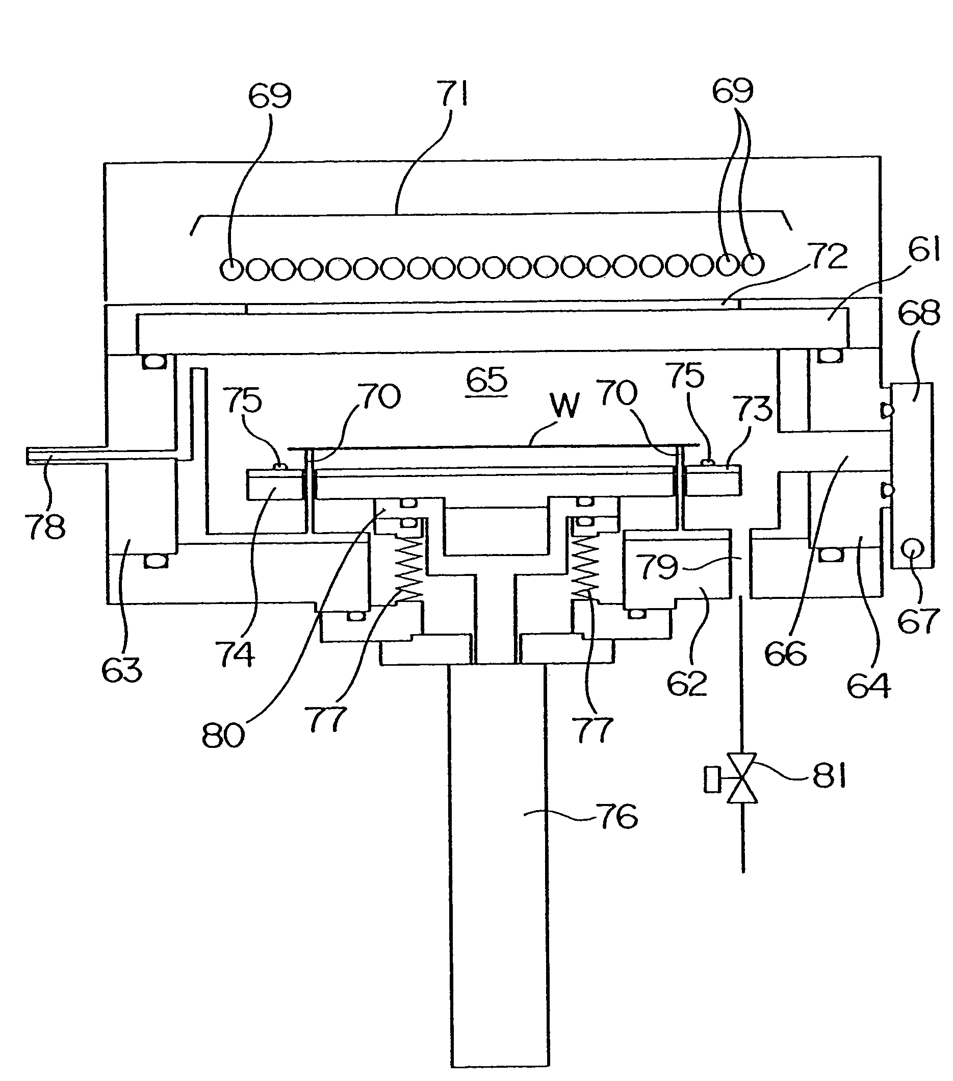
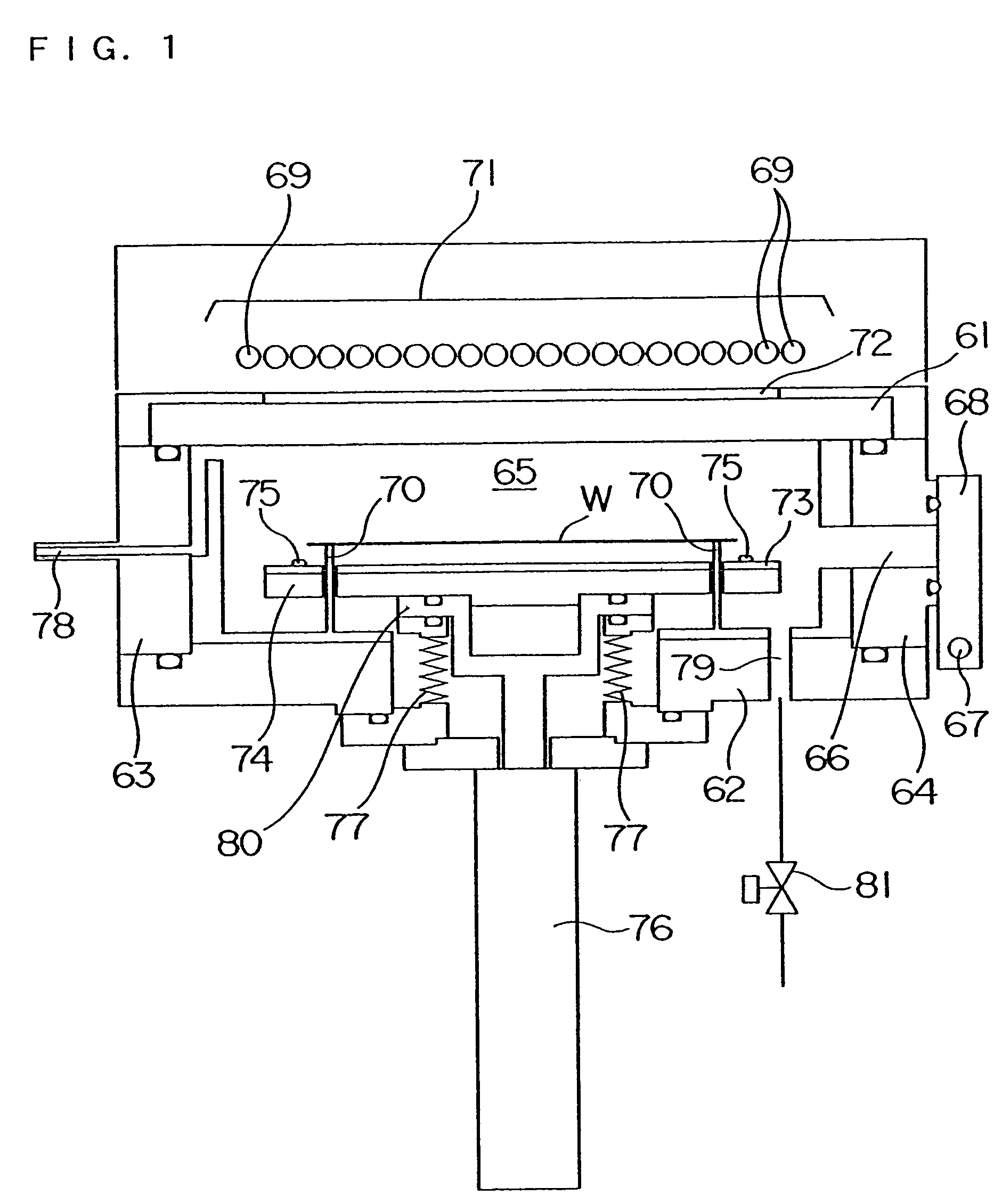
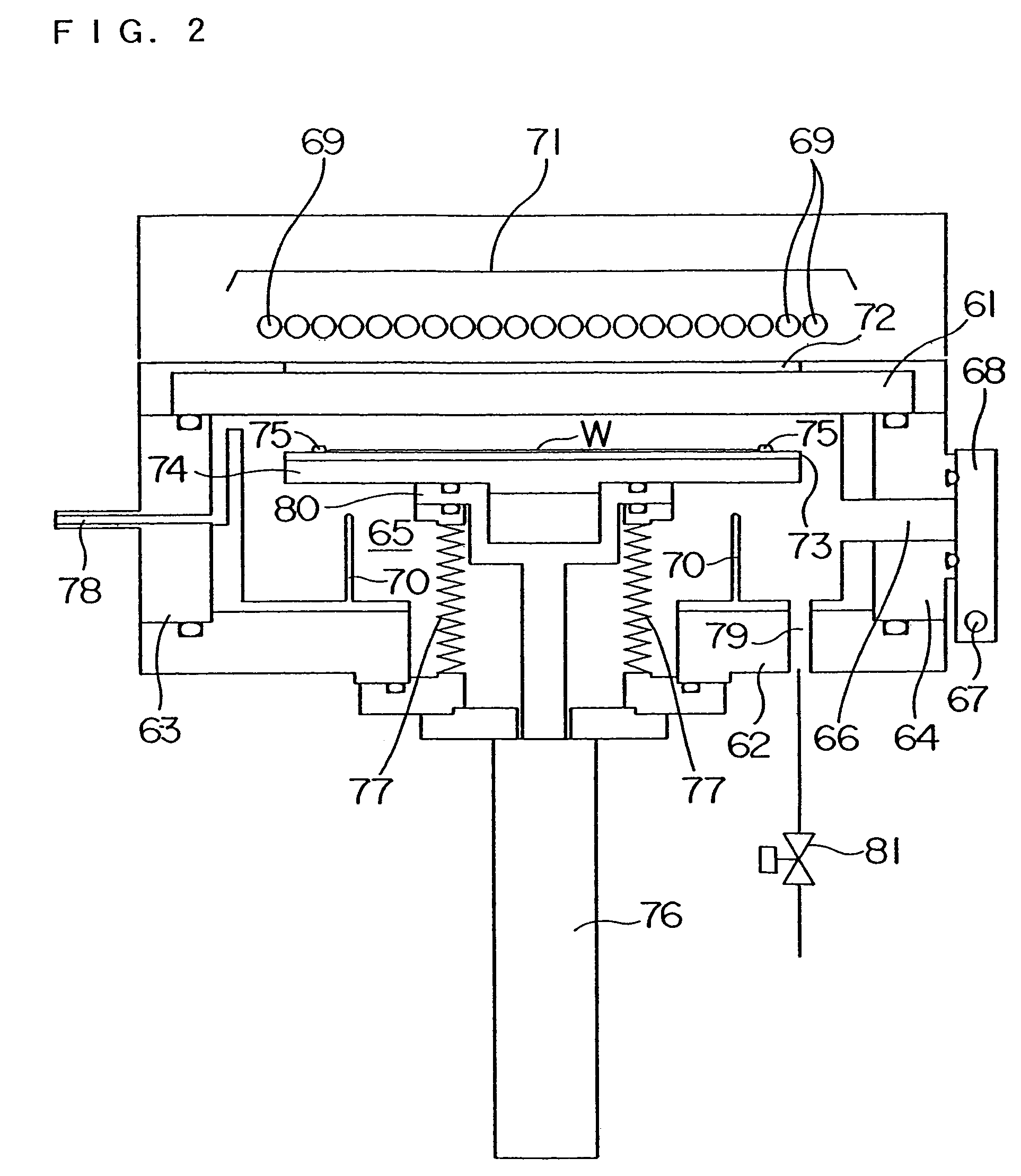
[0025]An embodiment of the present invention will be described hereinafter with reference to the drawings. FIGS. 1 and 2 are sectional side views of a heat treating apparatus according to the invention. FIG. 3 is a schematic plan view of the apparatus.

[0026]This heat treating apparatus includes a heat treating chamber 65 having a translucent plate 61, a bottom plate 62 and a pair of side plates 63 and 64 for receiving and heat treating a semiconductor wafer W. The translucent plate 61 acting as part of the heat treating chamber 65 is formed of an infrared transmitting material such as quartz. The bottom plate 62 acting as part of the heat treating chamber 65 has support pins 70 erected thereon and extending through a thermal diffuser plate 73 and a heating plate 74 to be described hereinafter, for supporting the semiconductor wafer W at the lower surface thereof.

[0027]The side plate 64 acting as part of the heat treating chamber 65 defines an opening 66 for loading and unloading the...


PUM

PropertyMeasurementUnit
temperatureaaaaaaaaaa
temperature T1aaaaaaaaaa
lighting timeaaaaaaaaaa

Abstract

A heat treating apparatus for heat treating a substrate by irradiating the substrate with light includes a heat treating chamber for receiving the substrate, a heating plate for preheating the substrate through a thermal diffuser plate, xenon flashlamps for heating the substrate preheated by the heating plate, to a treating temperature by irradiating the substrate with flashes of light, and a decompression mechanism for decompressing the heat treating chamber when the xenon flashlamps heat the substrate.

Description

CROSS REFERENCE TO A RELATED APPLICATION[0001]The present application is a Divisional Application of Ser. No. 10 / 267,127 filed Oct. 7, 2002, now abandoned which application claims the benefit and priority of Japanese Application Serial No. 2001-330230 filed Oct. 29, 2001, incorporated by reference.BACKGROUND OF THE INVENTION[0002]1. Field of the Invention[0003]The present invention relates to a heat treating apparatus and method for heat treating substrates such as semiconductor wafers by irradiating the substrates with light.[0004]2. Description of the Related Art[0005]A heat treating apparatus such as a lamp annealing apparatus with halogen lamps is used to execute a step of activating ions implanted in a semiconductor wafer. Such a heat treating apparatus activates ions in the semiconductor wafer by heating the wafer to a temperature of about 1,000 to 1,100 deg C., for example. Then, the heat treating apparatus heats the wafer at a rate of some several hundred degrees per second ...

Claims


Application Information

Patent Timeline
Patent Type & Authority Patents(United States)
IPC IPC(8): A21B2/00F27D11/02C30B31/12H01L21/00H01L21/26H01L21/324
CPCC30B31/12H01L21/324H01L21/67115
Inventor KUSUDA, TATSUFUMI
Owner DAINIPPON SCREEN MTG CO LTD
Learn More