

Electro-optical device and method of manufacturing the same
a technology of optical devices and optical components, applied in the field of semiconductor devices, can solve the problems of minute and complicated wiring patterns, dark display, blurred display,
- Summary
- Abstract
- Description
- Claims
- Application Information
AI Technical Summary
Benefits of technology
Problems solved by technology
Method used
Image

Examples
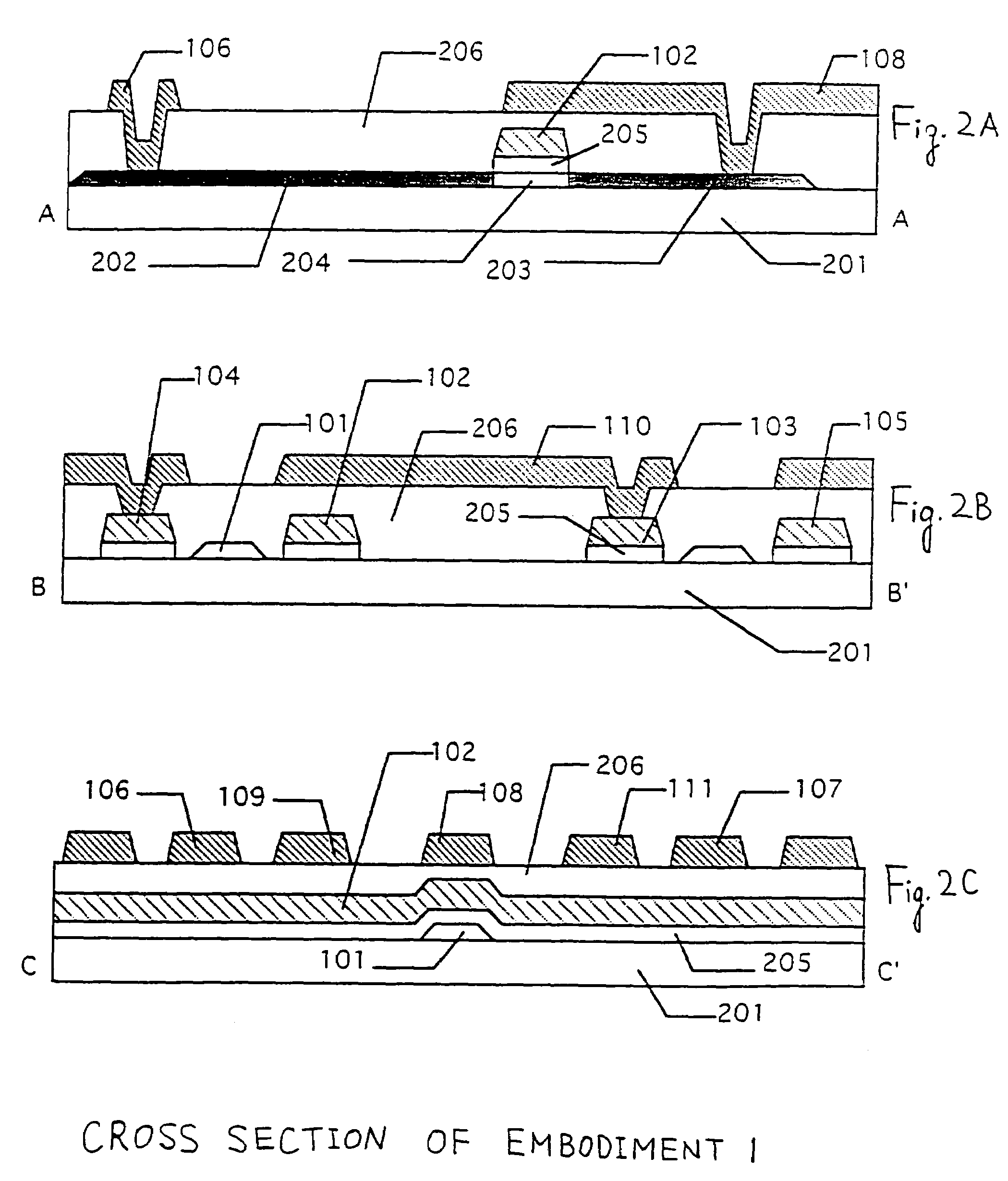
embodiment 1
[0117]Manufacturing steps of a liquid crystal display device according to this embodiment at a temperature of not higher than 600° C. will be described with reference to FIGS. 4 to 8.
[0118]A silicon oxide film with a thickness of 2,000 Å is grown as an under layer (not shown) on a substrate 201 (#1737 made by Corning) having an insulating surface by the sputtering method. In the case where a quartz substrate or the like is used, the under layer may not be grown.
[0119]Thereafter, an amorphous silicon film 101 with a thickness of 300 to 1,000 Å, in this embodiment, with a thickness of 500 Å is grown on the under layer of the silicon oxide by a parallel flat plate type plasma CVD method using glow discharge of silane. In the case where a low pressure CVD method is used, disilane is used to form an amorphous silicon film at a temperature of 450 to 650° C., typically 540° C. (FIG. 4A).
[0120]After the amorphous silicon film is formed, the amorphous silicon film is made to have crystallini...
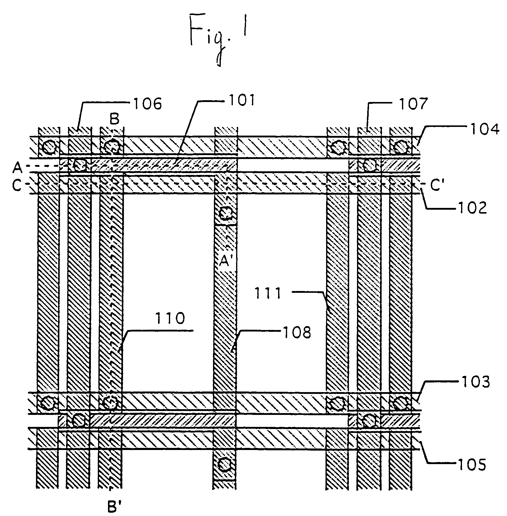
embodiment 2
[0159]In the structure of this embodiment, an electrode pattern is different from embodiment 1.
[0160]First, an under layer (not shown) and an amorphous silicon film are formed on a substrate having a insulating surface in the same manner as the embodiment 1.
[0161]After the amorphous silicon film is formed, like the embodiment 1, the amorphous silicon film is made to have crystallinity.
[0162]The thus obtained crystalline silicon film is shaped into an island region by the similar method as the embodiment 1. The shape of this crystalline silicon film is as shown in FIG. 11.
[0163]Further, a gate insulating film is deposited on the entire surface of the crystalline silicon film by the similar method to the embodiment 1.
[0164]Thereafter, an aluminum film as a first conductive film is deposited on the entire surface of the gate insulating film by the similar method to the embodiment 1.
[0165]Next, by using a resist mark formed on the first conductive film, the aluminum film and the gate in...
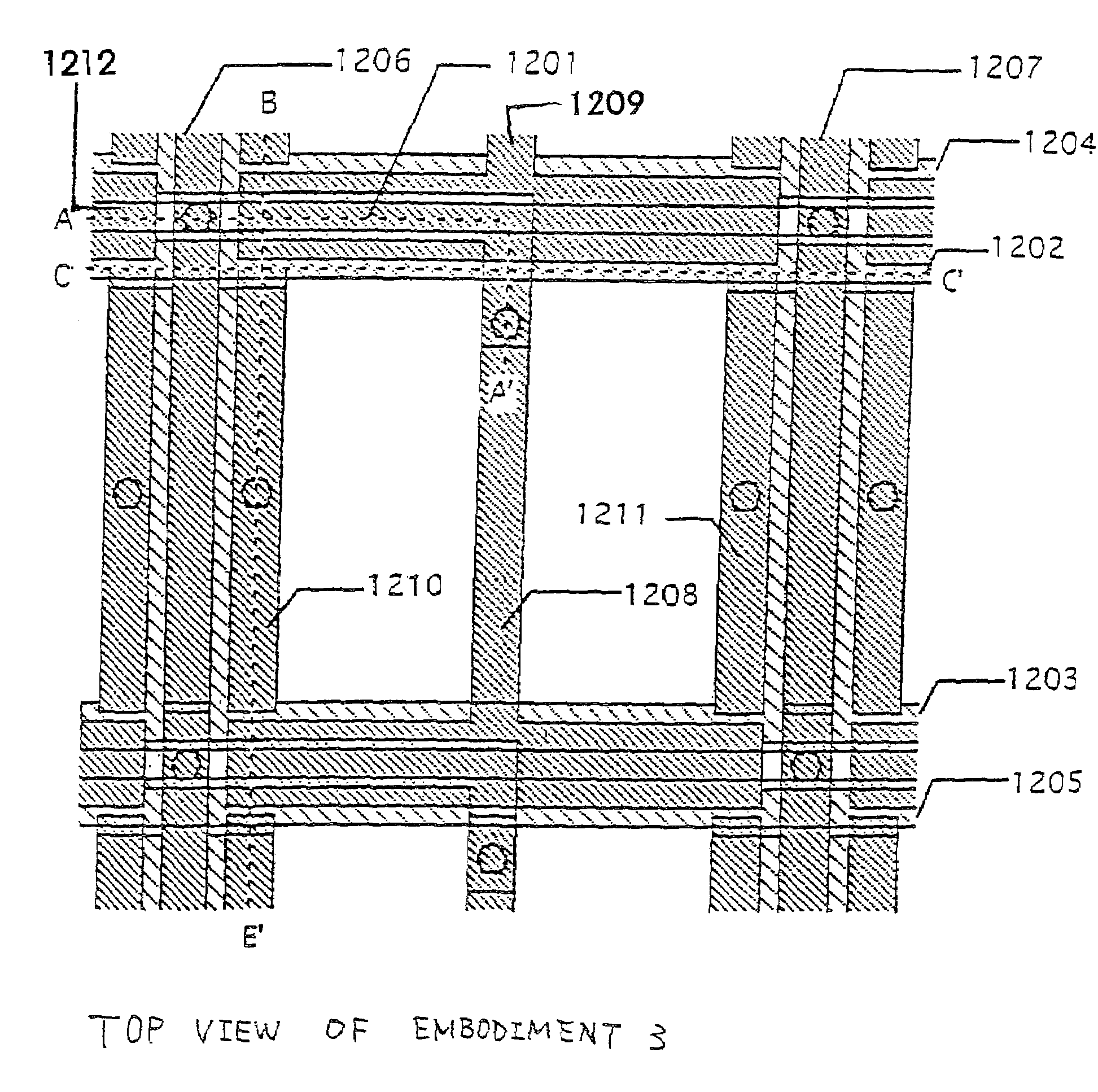
embodiment 3
[0177]The structure of this embodiment, as shown in FIGS. 12 and 13, is different from the embodiment 1 in a pixel electrode pattern, a common electrode pattern and an opposite substrate having a black matrix.
[0178]First, on a substrate having an insulating surface, an under film (not shown) and an amorphous silicon film are formed by the similar method to the embodiment 1.
[0179]After forming the amorphous silicon film, similar to the embodiment 1, the amorphous silicon film is made to have crystallinity.
[0180]The thus obtained crystalline silicon film is shaped into an island region 1201 by the similar method to the embodiment 1.
[0181]Further, a gate insulating film 1305 is deposited on the entire surface of the crystalline silicon film 1201 by the similar method to the embodiment 1.
[0182]Thereafter, an aluminum film as a first conductive film is deposited on the entire surface of the gate insulating film by the similar method to the embodiment 1.
PUM
| Property | Measurement | Unit |
|---|---|---|
| temperature | aaaaa | aaaaa |
| temperature | aaaaa | aaaaa |
| temperature | aaaaa | aaaaa |
Abstract
Description
Claims
Application Information