Method of synthesising and growing nanorods from a metal carbide on a substrate, substrates thus obtained and applications thereof

a metal carbide and nanorod technology, applied in the direction of crystal growth process, ion implantation coating, chemical vapor deposition coating, etc., can solve the problem of nanotubes that are not attached to any substrate, inability to produce nano-objects of the type of nanotubes or nanorods over large areas, and inability to use these processes. achieve the effect of high degree of gas dissociation

Inactive Publication Date: 2008-03-04
COMMISSARIAT A LENERGIE ATOMIQUE ET AUX ENERGIES ALTERNATIVES
View PDF4 Cites 12 Cited by
  • Summary
  • Abstract
  • Description
  • Claims
  • Application Information

AI Technical Summary

Benefits of technology

[0050]It is thus possible to carry out all the steps of the synthesis process according to the invention by means of one and the same device, namely an ECR microwave plasma source, this being a further advantage of the invention.
[0051]This ECR microwave plasma source is preferably a source with high magnetic confinement of the type described in document [11], allowing the generation of low-pressure plasmas with highly energetic electrons and thereby ensuring a very high degree of dissociation of the gases in the plasma chamber.
[0052]With regard to the foregoing, the metal M1 is preferably chosen from metals capable of reacting, in step c), with organic molecules or radicals that are in gaseous form in order to form, with them, a metal carbide and thus induce the growth of nanorods made of this carbide from the nanocrystals of this metal M1.
[0053]Metals of this type are especially chromium and molybdenum, chromium being preferred within the context of the invention.
[0054]The metal or metals M2 are chosen from metals having an affinity for carbon-containing molecules or radicals that are in gaseous form, which allows them, in step c) to fix these molecules or radicals by metal-carbon bonds and makes it possible to form a protective graphitic layer that blocks any growth from the nanocrystals of this or these metals M2.
[0055]Such metals are those known as catalysts in organic chemistry. They are in particular iron, nickel and cobalt, iron and nickel being preferred within the context of the invention.

Problems solved by technology

First, there are those which are aimed at producing nanotubes on powders of catalyst crystals and which result in the formation of nanotubes that are not attached to any substrate.
Because the processes described in documents [5] to [8] include a lithography operation, which is extremely expensive and can be carried out only over limited areas, the use of these processes is inconceivable for the production of nano-objects of the nanotube or nanorod type over large areas.
In addition, the dispersion of the nanotubes on the surface of the substrate proves to be highly irregular in the case of document [6], whereas it is non-existent in the case of document [8], because the latter case results in the formation of nanotubes joined together in bundles.
Although this process has the advantage of not using lithography, it does not make it possible, however, to obtain a uniform distribution of the nanotubes and with a sufficient spacing between the latter.
However, the distance between these channels cannot be easily controlled and, here again, the nanotubes obtained are insufficiently far apart.
Thus, the only processes at the present time that allow the production, on a substrate, of vertically erect nano-objects separated from one another all include a lithography operation, which is both expensive and limited to small areas.

Method used


Image

  • Method of synthesising and growing nanorods from a metal carbide on a substrate, substrates thus obtained and applications thereof
  • Method of synthesising and growing nanorods from a metal carbide on a substrate, substrates thus obtained and applications thereof
  • Method of synthesising and growing nanorods from a metal carbide on a substrate, substrates thus obtained and applications thereof

Examples


example 1

Synthesis of Chromium Carbide Nanorods on Silicon

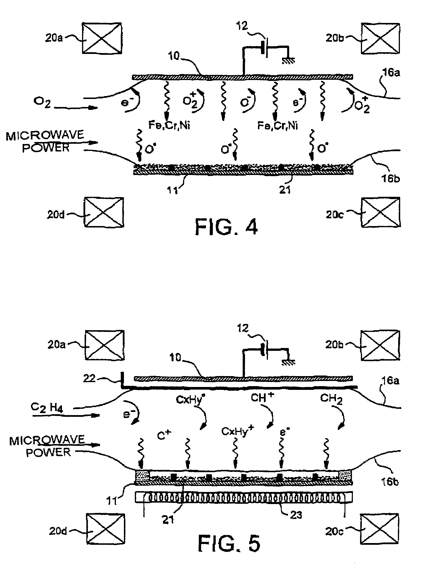
[0112]Chromium carbide nanorods were synthesized on silicon substrates using, for the three steps a), b) and c), an ECR microwave plasma source with high magnetic confinement, similar to that described in document [11].

[0113]The operating conditions were the following:[0114]step a): sputtering of a metal target by an oxygen plasma:[0115]target used: austenitic stainless steel composed of 68% Fe, 18% Cr and 14% Ni[0116]target bias: −400 V[0117]oxygen pressure: 2×10⁻⁴ mbar[0118]sputtering time: 20 minutes[0119]thickness of the nanocrystal layer thus deposited:≈50 nm;[0120]step b): reduction by a hydrogen plasma:[0121]hydrogen pressure: 1.5×10⁻³ mbar[0122]substrate temperature: 500° C.[0123]reduction time: 10-20 minutes;[0124]step c): growth by an ethylene plasma:[0125]microwave power: 50-150 watts for a frequency of 2.45 GHz[0126]ethylene pressure: 10−3−3 ×10⁻³ mbar[0127]substrate temperature: 640° C.[0128]growth time: 10-30 minutes.

[01...

example 2

Synthesis of Chromium Carbide Nanorods on a Stainless Steel Grid

[0132]Chromium carbide nanorods were synthesized on a substrate consisting of a stainless steel grid, also using, for the three steps a), b) and c), an ECR microwave plasma source with high magnetic confinement, similar to that described in document [11].

[0133]The operating conditions were the following:[0134]step a): sputtering of a metal target by an oxygen plasma:[0135]target used: austenitic stainless steel composed of 68% Fe, 18% Cr and 14% Ni[0136]target bias: −400 V[0137]oxygen pressure: 2×10⁻⁴ mbar[0138]sputtering time: 20 minutes[0139]thickness of the nanocrystal layer thus deposited:≈50 nm;[0140]step b): reduction by a hydrogen plasma:[0141]hydrogen pressure: 3×10⁻³ mbar[0142]substrate temperature: 550° C.[0143]reduction time: 10 minutes;[0144]step c): growth by an ethylene plasma:[0145]microwave power: 50 watts for a frequency of 2.45 GHz[0146]ethylene pressure: 3×10⁻³ mbar[0147]substrate temperature: 620° C....


PUM

PropertyMeasurementUnit
voltageaaaaaaaaaa
voltageaaaaaaaaaa
pressureaaaaaaaaaa

Abstract

The invention relates to a process for synthesizing nanorods of a carbide of one metal M1 on a substrate, which comprises:a) the deposition, on the substrate, of a layer of nanocrystals of oxide of the metal M1 and nanocrystals of oxide of at least one metal M2 different from metal M1, the M1 metal oxide nanocrystals being dispersed within this layer;b) the reduction of the M1 and M2 metal oxide nanocrystals into corresponding metal nanocrystals; andc) the selective growth of the M1 metal nanocrystals.The invention also relates to a process for growing nanorods of a carbide of one metal M1 on a substrate from nanocrystals of this metal, to the substrates thus obtained and to their applications: fabrication of Microsystems provided with chemical or biological functionalities, in particular the fabrication of biosensors; electron emission sources, for example for flat television or computer screens; etc.

Description

TECHNICAL FIELD[0001]The invention relates to a process for synthesizing metal carbide nanorods on a substrate, and more particularly chromium carbide nanorods, and to a process for growing such nanorods on a substrate from nanocrystals of the same metal.[0002]It furthermore relates to the substrates thus obtained and to their applications.[0003]The synthesis and growth processes according to the invention result in the formation of metal carbide nanorods which, apart from having a rigid and robust structure inherent in carbides, are firmly attached to the substrate on which their synthesis or their growth was carried out, perpendicular to the principal plane of this substrate, and are physically separate from one another, i.e. are not in contact with one another.[0004]These nanorods are therefore capable of being functionalized by the grafting of organic, chemical or biological molecules and consequently are of most particular benefit for the fabrication of microsystems provided wi...

Claims


Application Information

Patent Timeline
Patent Type & Authority Patents(United States)
IPC IPC(8): C30B1/02C01B31/30C01B32/949C23C14/00C23C14/08C23C14/58C30B29/66
CPCB82Y30/00C01B31/303C23C14/0036C23C14/08C23C14/58C23C14/5846C01P2004/13C01P2004/64C01P2004/82C01B32/914
Inventor DELAUNAY, MARCVINET, FRANCOISE
Owner COMMISSARIAT A LENERGIE ATOMIQUE ET AUX ENERGIES ALTERNATIVES
Why Eureka
Try Eureka