Check patentability & draft patents in minutes with Patsnap Eureka AI!

Semiconductor device and manufacturing method thereof

a semiconductor and semiconductor technology, applied in semiconductor devices, semiconductor/solid-state device details, electrical devices, etc., can solve the problems of reducing the yield, warping of the wafer, and the inability to obtain semiconductor chips of a uniform thickness, so as to save the cost

Inactive Publication Date: 2008-04-15
ROHM CO LTD
View PDF21 Cites 16 Cited by
  • Summary
  • Abstract
  • Description
  • Claims
  • Application Information

AI Technical Summary

Benefits of technology

This approach enables uniform thickness and high-strength semiconductor chips with reduced warping, enhanced reliability, shorter manufacturing time, and miniaturization capabilities by managing thermal stress and preventing electrical short-circuits.

Problems solved by technology

Hence, if a reduction in thickness is pursued excessively, breaking occurs in the wafer and the chips when handled, and as a consequence, the yield is lowered.
The above-described manufacturing method of the related art, however, has a problem that, as shown in FIG. 6 exaggeratedly, warping occurs in the wafer during a period since the resin film was formed on the surface of the wafer until the backside grinding is performed due to a difference in thermal expansion / contraction coefficient between the wafer and the resin film.
Grinding a wafer having warping with a flat grinding wheel yields a difference in thickness between the central region and the edge region of the ground wafer, which makes it impossible to obtain semiconductor chips of a uniform thickness.
Moreover, the semiconductor chips cut away from the edge portion of the wafer may not be reduced to a target thickness.
However, because the wafer is cut by a thin grinding wheel (20 to 100 μm) called a blade during the dicing process, flaws called chipping or microcracking occur at the corners of the diced pieces.
In this instance, however, the needle or the like damages the semiconductor substrate, and deteriorates the quality considerably.
Also, the fabricated semiconductor device is exposed at the back surface on the side opposite to the active surface of the semiconductor substrate, and is therefore fragile and less reliable.
However, in a case where the semiconductor substrate, such as a semiconductor wafer and a semiconductor chip, is made of silicon, for example, and the resin film is made of epoxy resin, for example, there is a considerable difference in thermal expansion coefficient between the semiconductor substrate and the resin film.
For these reasons, when the semiconductor substrate and the resin film undergo thermal expansion / contraction during the fabrication sequence or operations of the semiconductor device, the posts together with the resin film cause displacement, and considerable shearing stress is applied to a junction portion between the posts and the electrode pads, which may result in breaking of an electrical connection between the posts and the electrode pads.
However, in the case of forming the posts through plating, because a time needed for the plating is nearly proportional to the length of the posts, it takes a considerable time to form long posts, and as a result, a long manufacturing time is needed for a semiconductor device.
Further, because copper is an element that readily migrates, for example, in a case where the resin film is made of polyimide that readily absorbs moisture, if neighboring posts are formed too close, these posts electrically short-circuit due to migration.
Hence, a wide space needs to be secured between neighboring posts, which is a factor that makes miniaturization of the semiconductor device difficult.

Method used


Image

  • Semiconductor device and manufacturing method thereof
  • Semiconductor device and manufacturing method thereof
  • Semiconductor device and manufacturing method thereof

Examples


first embodiment

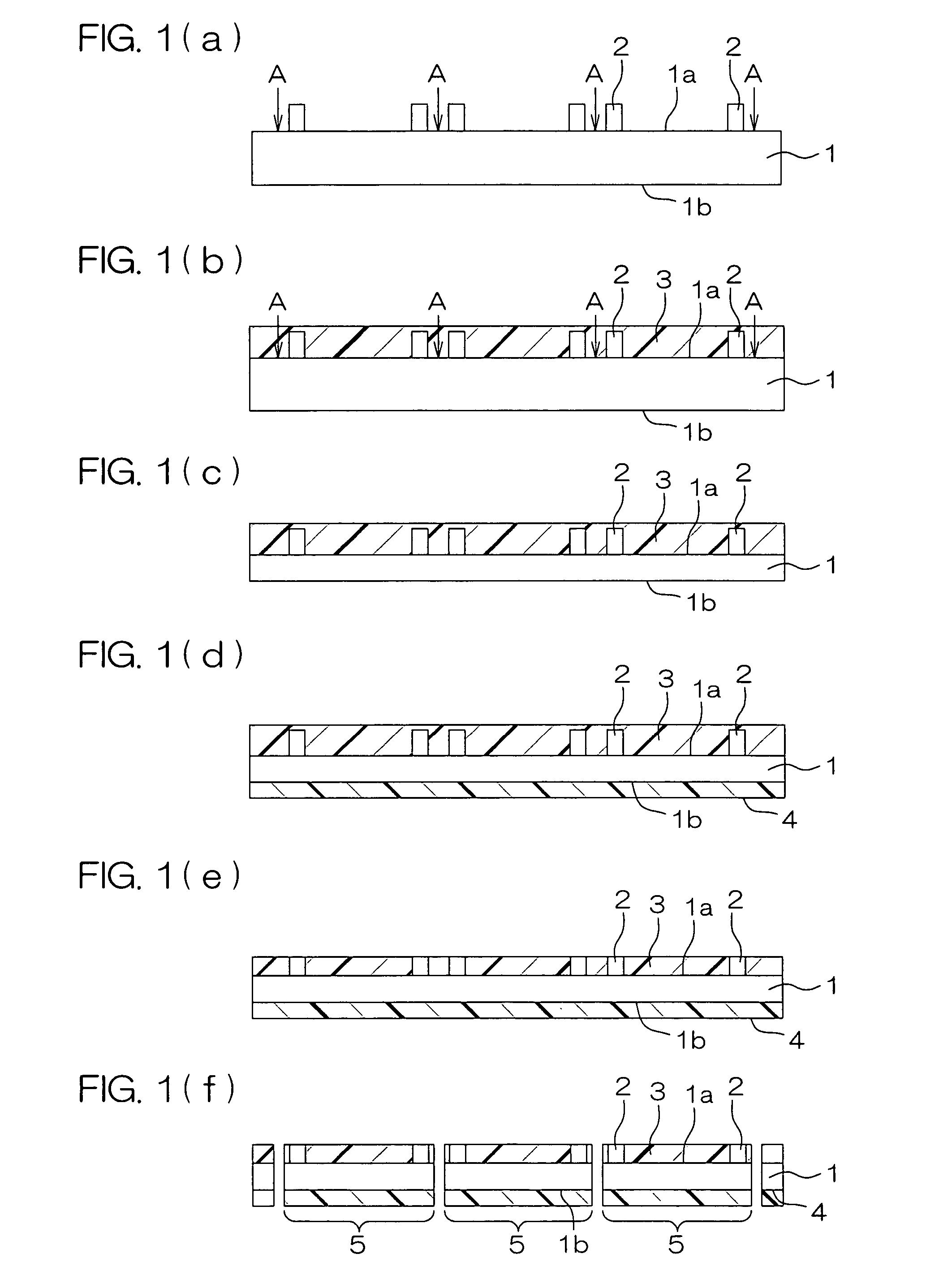
[0046]FIGS. 1(a) through 1(f) are schematic cross sections showing a step-by-step manufacturing method of a semiconductor device according to the invention. A semiconductor wafer 1 (hereinafter, referred to simply as the wafer 1) of the drawings has undergone the forming process of various elements and the wiring process, and a surface 1a, which is a surface on an active surface layer region side, is covered with a passivation film made of a nitride film or the like. Pads used to establish an external electrical connection are exposed from the passivation film.

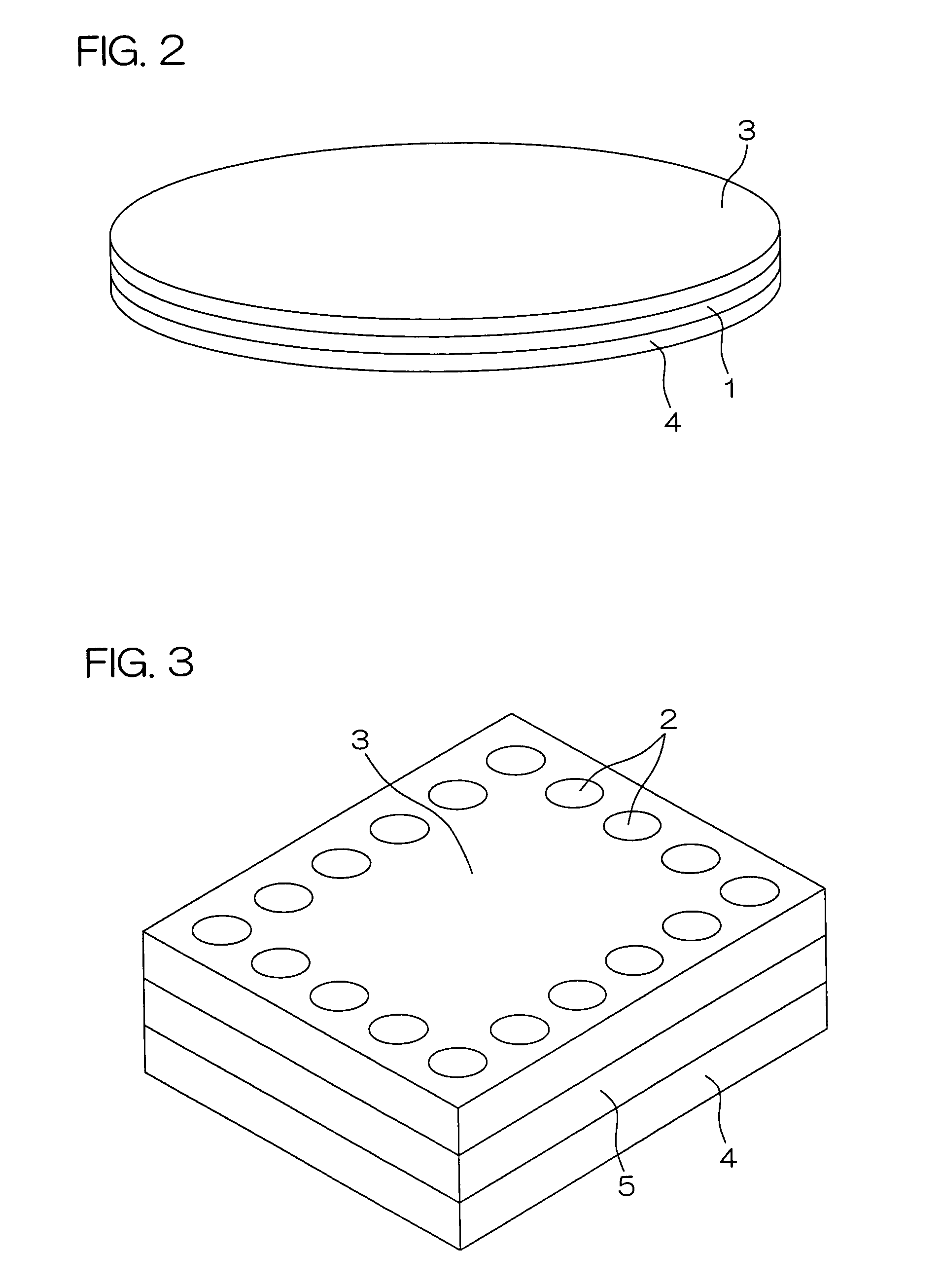
[0047]As shown in FIG. 1(a), a plurality of protruding electrodes 2 made of gold (Au), for example, are formed on the pads. The protruding electrodes 2 are formed, for example, through electrolytic plating, and it is preferable to set a height thereof from the surface of the passivation film to 50 μm approximately. The protruding electrodes 2 are preferably shaped like a pillar, such as a cylindrical pillar and a prismatic pil...

second embodiment

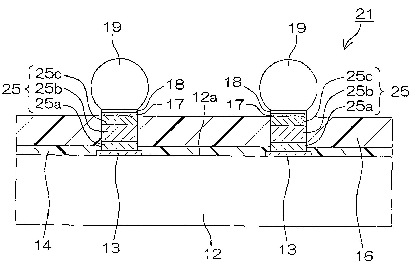
[0059]FIG. 4 is a schematic cross section showing a semiconductor device 11 according to the invention.

[0060]The semiconductor device 11 includes a semiconductor chip 12. In the semiconductor chip 12, redistribution wiring including electrode pads 13 is formed on an active surface 12a on which circuits are formed. The electrode pads 13 are made of copper (Cu). A passivation film 14 is formed on the redistribution wiring in such a manner that the electrode pads 13 are exposed. A resin film 16 is formed on the passivation film 14.

[0061]A post (for example, a cylindrical pillar-shaped electrode) 15 made of gold (Au) is bonded to each electrode pad 13 almost vertically. The posts 15 are provided to penetrate through the resin film 16. A nickel (Ni) layer 17 is formed on the tip end (on the opposite side to the junction portion with the electrode pad 13) of each post 15, and a thin gold flash layer 18 (for example, a thickness of 0.5 μm approximately) is formed on the nickel layer 17 to ...


PUM

PropertyMeasurementUnit
elastic modulusaaaaaaaaaa
thicknessaaaaaaaaaa
thicknessaaaaaaaaaa

Abstract

A semiconductor device having a semiconductor substrate, at least one of a protruding electrode and wiring formed on one surface of the semiconductor substrate, and a first resin film formed on this surface. The first resin film has elasticity low enough to reduce stress induced by a difference in thermal expansion coefficient between the semiconductor substrate and the first resin film. A second resin film, having higher elasticity or higher strength than the first resin film, may be formed on the other surface of the semiconductor substrate.

Description

BACKGROUND OF THE INVENTION[0001]1. Field of the Invention[0002]The present invention relates to a miniaturized, thin semiconductor device and a manufacturing method thereof.[0003]2. Description of Related Arts[0004]In the effort of reducing a semiconductor chip in thickness, there has been performed a backside grinding process for grinding the back surface side of a semiconductor wafer (hereinafter, referred to simply as the wafer) on which elements and wiring are already formed. The backside grinding process is generally performed by laminating a soft protection film on the surface of the wafer, and then by rotating the wafer while pressing the back surface of the water against a grinding wheel with pressure being applied to the wafer through the protection film.[0005]However, during the processes subsequent to the grinding, for example, the dicing process for cutting individual chips away from the wafer and the mounting process for mounting the diced chips onto a lead frame, the ...

Claims


Application Information

Patent Timeline
Patent Type & Authority Patents(United States)
IPC IPC(8): H01L23/29H01L21/301H01L23/31H01L23/485
CPCH01L23/3114H01L24/10H01L24/13H01L2924/0002H01L2224/0401H01L2224/13099H01L2924/01029H01L2924/01078H01L2924/01079H01L2924/01082H01L2924/14H01L2924/3511H01L2224/13023H01L2924/01005H01L2924/01006H01L2924/01033H01L2924/014H01L2224/05568H01L2924/00H01L2224/05552H01L2224/13H01L2224/05144H01L2224/05147H01L2224/05155H01L2224/05644H01L2224/05647H01L24/05H01L2924/00014
Inventor SHIBATA, KAZUTAKA
Owner ROHM CO LTD
Features
  • R&D
  • Intellectual Property
  • Life Sciences
  • Materials
  • Tech Scout
  • Unparalleled Data Quality
  • Higher Quality Content
  • 60% Fewer Hallucinations
Learn More