

Nonvolatile semiconductor memory
a semiconductor memory and non-volatile technology, applied in the field of non-volatile semiconductor memory, can solve the problems of loss of product competitiveness, the current process technology for implementing miniaturized nand flash eeprom cannot keep up, and the process technology is always being pursued to the limit of process technology
- Summary
- Abstract
- Description
- Claims
- Application Information
AI Technical Summary
Benefits of technology
Problems solved by technology
Method used
Image

Examples
first embodiment
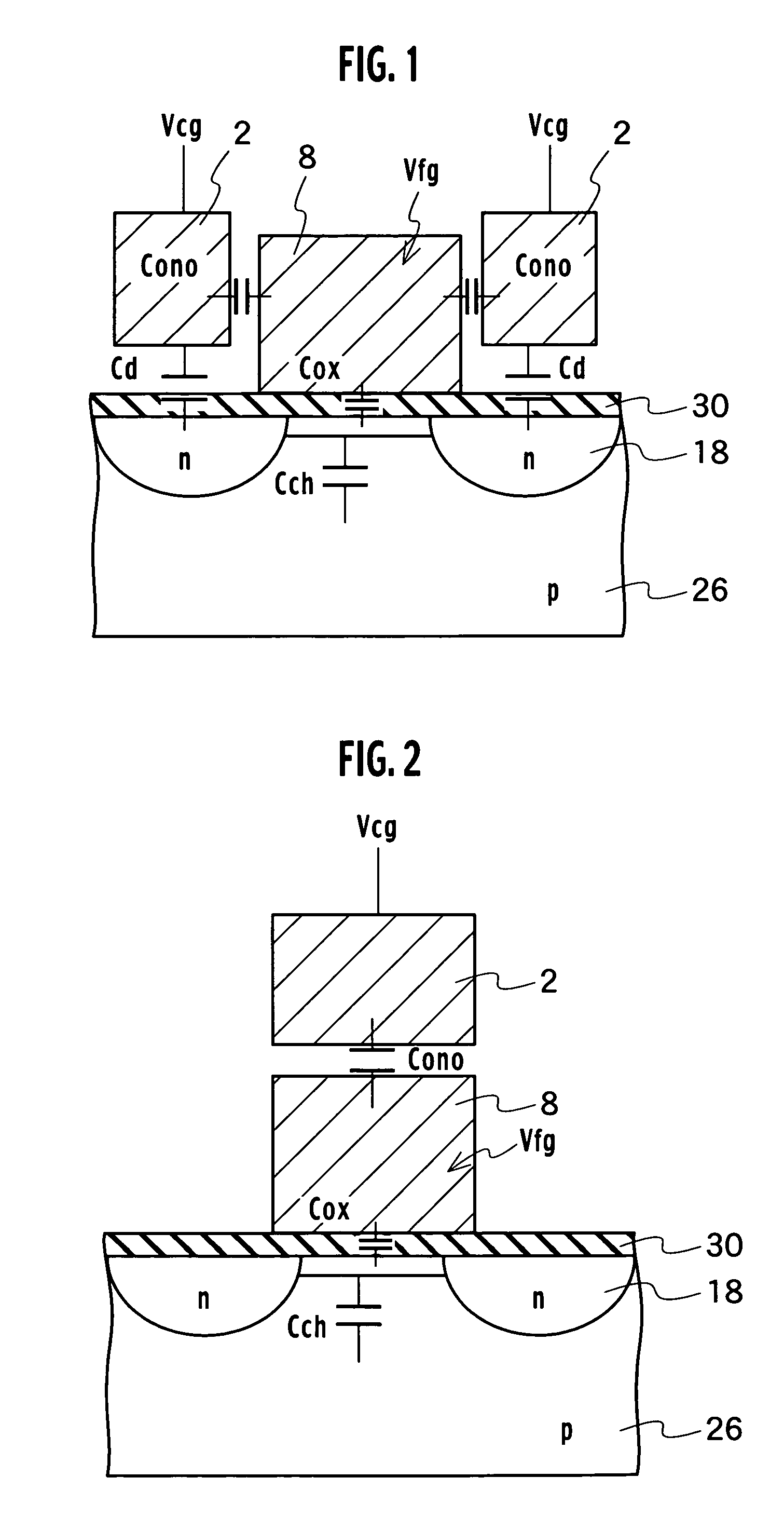
[0082]The basic structure of a memory cell transistor of a nonvolatile semiconductor memory according to a first embodiment of the present invention is, as shown in FIG. 1, a sidewall control gate structure including diffusion layers 18 formed in a semiconductor substrate 26 to be a source region or a drain region, a tunneling insulator film 30 formed on the semiconductor substrate 26, a floating gate 8 formed on a channel region sandwiched between the diffusion layers 18 via the tunneling insulator film 30, a first and second control gates 2 formed adjacent to the two sidewalls of the floating gate 8 via an inter-gate insulator film 40 and facing the diffusion layers 18 that will be a source or a drain.
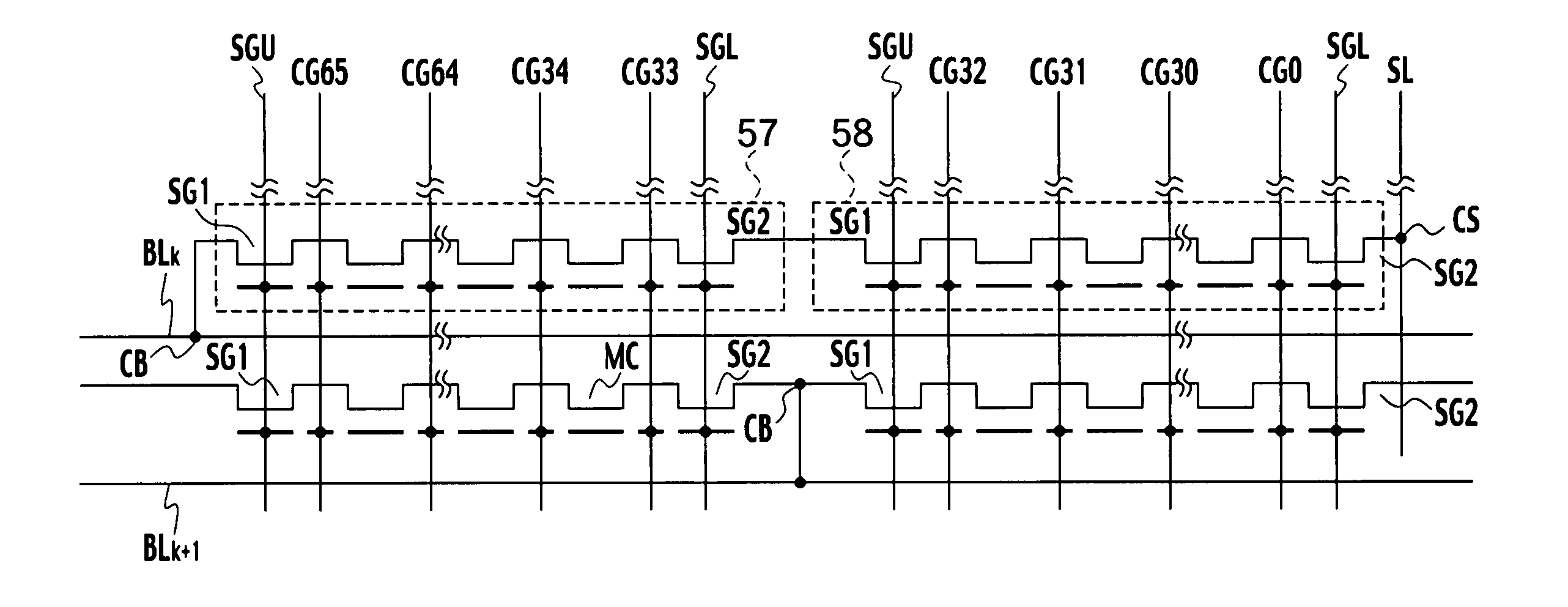
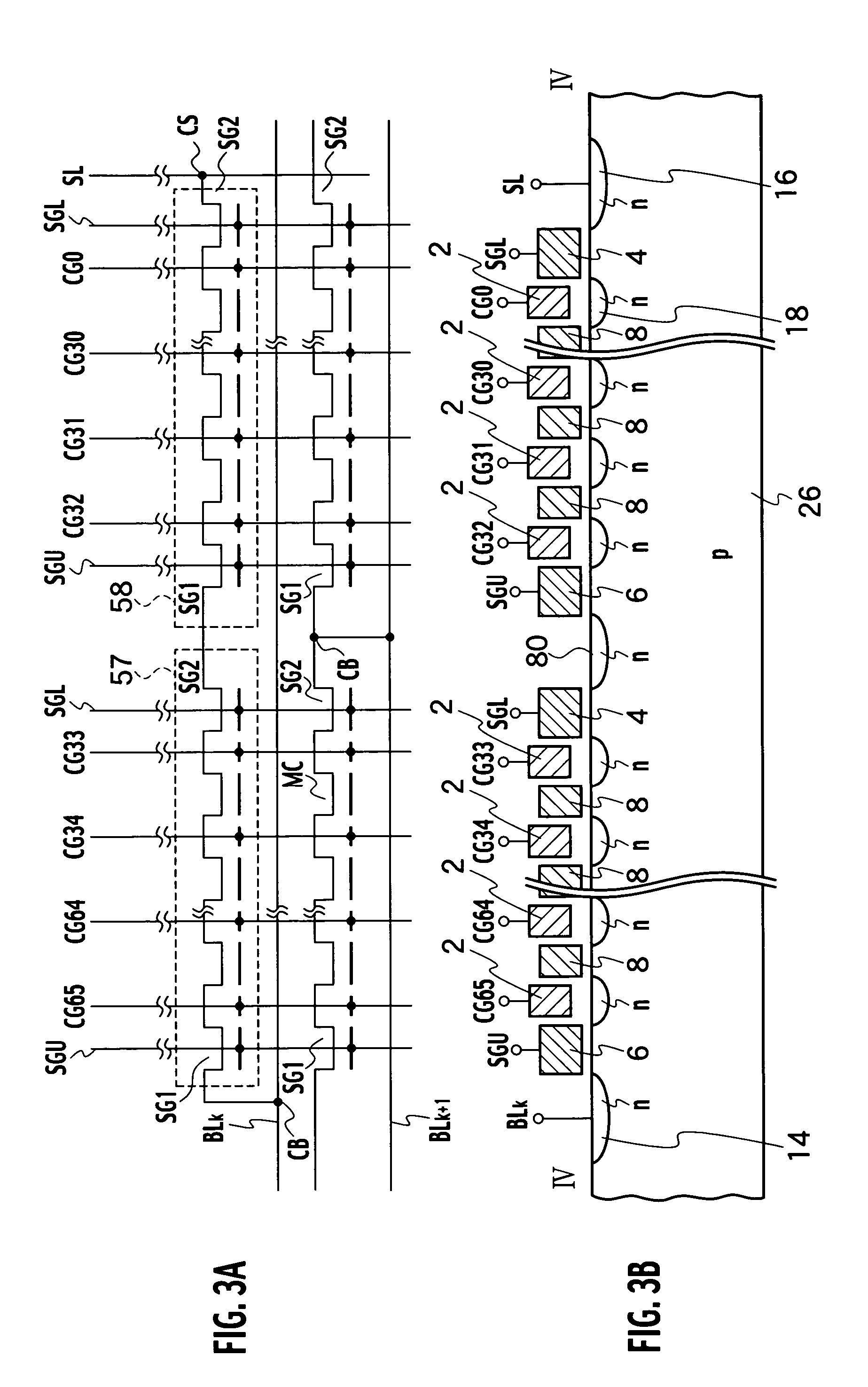
[0083]The nonvolatile semiconductor memory according to the embodiments of the present invention with the sidewall control gate structure as a basic structure has circuitry and a device cross-sectional structure as shown in FIGS. 3A and 3B. Memory cell transistors MC have a sidewall ...
second embodiment
[0104]The basic structure of a memory cell transistor of a nonvolatile semiconductor memory according to the second embodiment of the present invention is, as shown in FIG. 2, a stacked structure including: diffusion layers 18 formed in a semiconductor substrate 26 to be a source region or a drain region; a tunneling insulator film 30 formed on the semiconductor substrate 26; a floating gate 8 formed upon a channel region sandwiched between the diffusion layers 18 via the tunneling insulator film 30; and a control gate 2 formed on the floating gate 8 via an interlayer insulator film.
[0105]According to the sidewall control gate structure, the parasitic capacitance around the floating gate 8 can be reduced, and increasing the value of the capacitance between the control gate 2 and the floating gate 8 allows a decrease in the write-in voltage Vpgm and provides a nonvolatile semiconductor memory capable of dense integration and high-speed performance. On the other hand, two control gate...
first modified example
(First Modified Example of Write-in Mode)
[0114]In order to cut off the select gate transistors SG1 and SG2, a back bias voltage is transferred to the inter-unit diffusion layer 80 via neighboring memory cell block regions 62. At this time, pass voltages (DC) are applied to the word lines WL for the neighboring memory cell block regions 62. However, read disturb may be worsened.
PUM
 Abstract
Description
Claims
Application Information