Preparation of metal chalcogenides from reactions of metal compounds and chalcogen

a technology of metal chalcogenide and reaction reaction, which is applied in the field of synthesis of metal chalcogenide, can solve the problems of inability to efficiently obtain ssup>0/sup>, inability to efficiently use hsup>2/sub>s alone, and inability to achieve hsup>2/sub>s at low temperatures

Inactive Publication Date: 2008-07-01
ARIZONA STATE UNIVERSITY
View PDF13 Cites 45 Cited by
  • Summary
  • Abstract
  • Description
  • Claims
  • Application Information

AI Technical Summary

Benefits of technology

[0011]In another embodiment, there is disclosed a method of preparing indium sulfide (In2S3) from In2O3. The method includes providing boron, pure sulfur, and pure In2O3; placing the boron and the sulfur in a first tube; placing the In2O3 in a second tube; placing the two tubes into a larger container; sealing the container; gradually heating the container to about 400-900° C.; keeping the container at that temperature for about two days or until little boron remains; and allowing the container to cool.

Problems solved by technology

For example, the synthesis of metal polysulfides has not been straightforward by the existing methods because many polysulfides decompose at elevated temperatures and the sources of the polyanions are relatively scarce.
H2S alone is not an efficient source of S0, and the thermodynamics of the thermal decomposition of H2S are not favorable at low temperatures.
FeS2 and CoS2 have also been prepared at higher temperatures by reacting H2S with starting materials that contain the corresponding metal ions of high oxidation states, but the problem of incomplete reactions and / or of impurities still remains.

Method used


Image

  • Preparation of metal chalcogenides from reactions of metal compounds and chalcogen
  • Preparation of metal chalcogenides from reactions of metal compounds and chalcogen
  • Preparation of metal chalcogenides from reactions of metal compounds and chalcogen

Examples


example 1

Formation of NdS2 Polysulfide Nanoparticles from Nd2O3 Nanoparticles

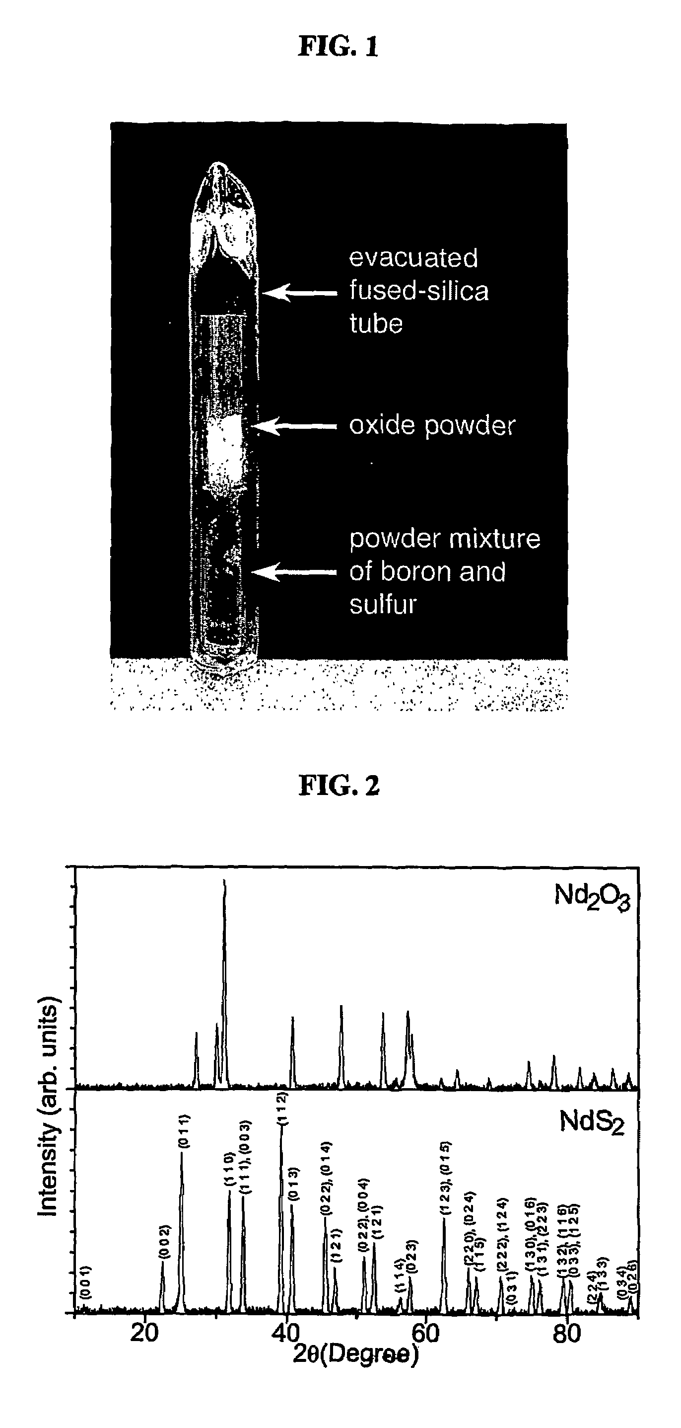
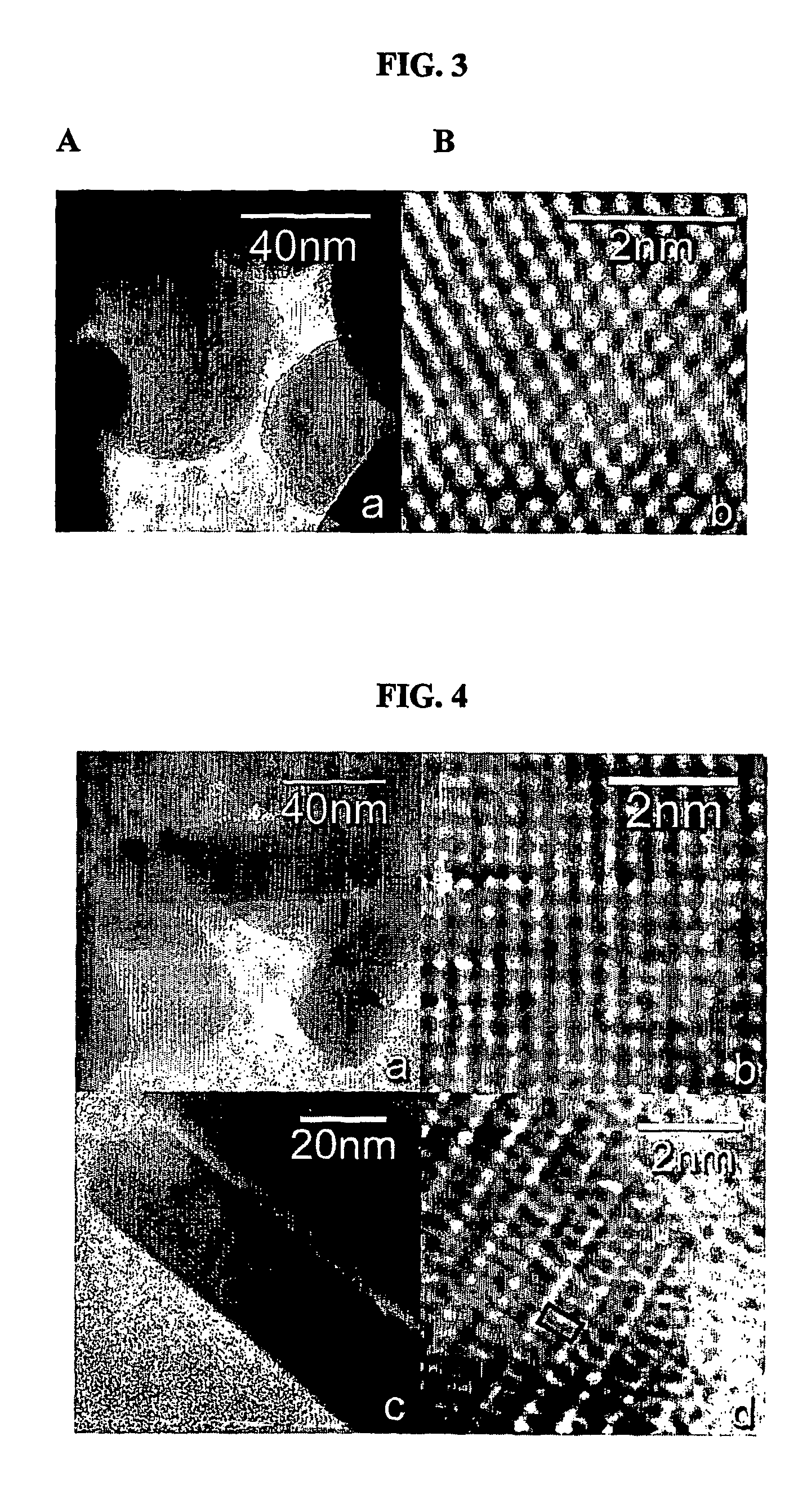
[0058]First, 0.337 g (1 mmol) of Nd2O3 powder (99.9%, 49-64 nm, Nanostructured & Amorphous Materials Inc., Los Alamos, N. Mex.) was placed in a short fused silica tube (FIG. 1). Excess amounts of amorphous boron (99.99%, 325 mesh, Alfa Aesar, Ward Hill, Mass.) and sulfur powders (99.999%, Alfa Aesar) were mixed in the molar ratio of 1:4 and placed in a separate fused silica tube of the same size. The two tubes were subsequently situated inside a larger silica tube container, with the tube of Nd2O3 on top of the other. After the whole container was evacuated and flame-sealed, it was gradually heated to 450° C., kept at the temperature for one day, and radiatively cooled to room temperature. The pale violet color of the original oxide powder turned into grayish yellow after the reaction. The silica reaction tubes were intact, with no visible corrosion on the inner surface of the tubes. FIG. 2 compares the powder x-ray...

example 2

Conversion of the Nanoparticles of Rare-Earth Oxides (Tb4O7, Ce2O3, Sm2O3, Er2O3 and Eu2O3) into the Nanoparticles of their Corresponding Disulfides (TbS2, CeS2, SmS2, ErS2 and EuS2)

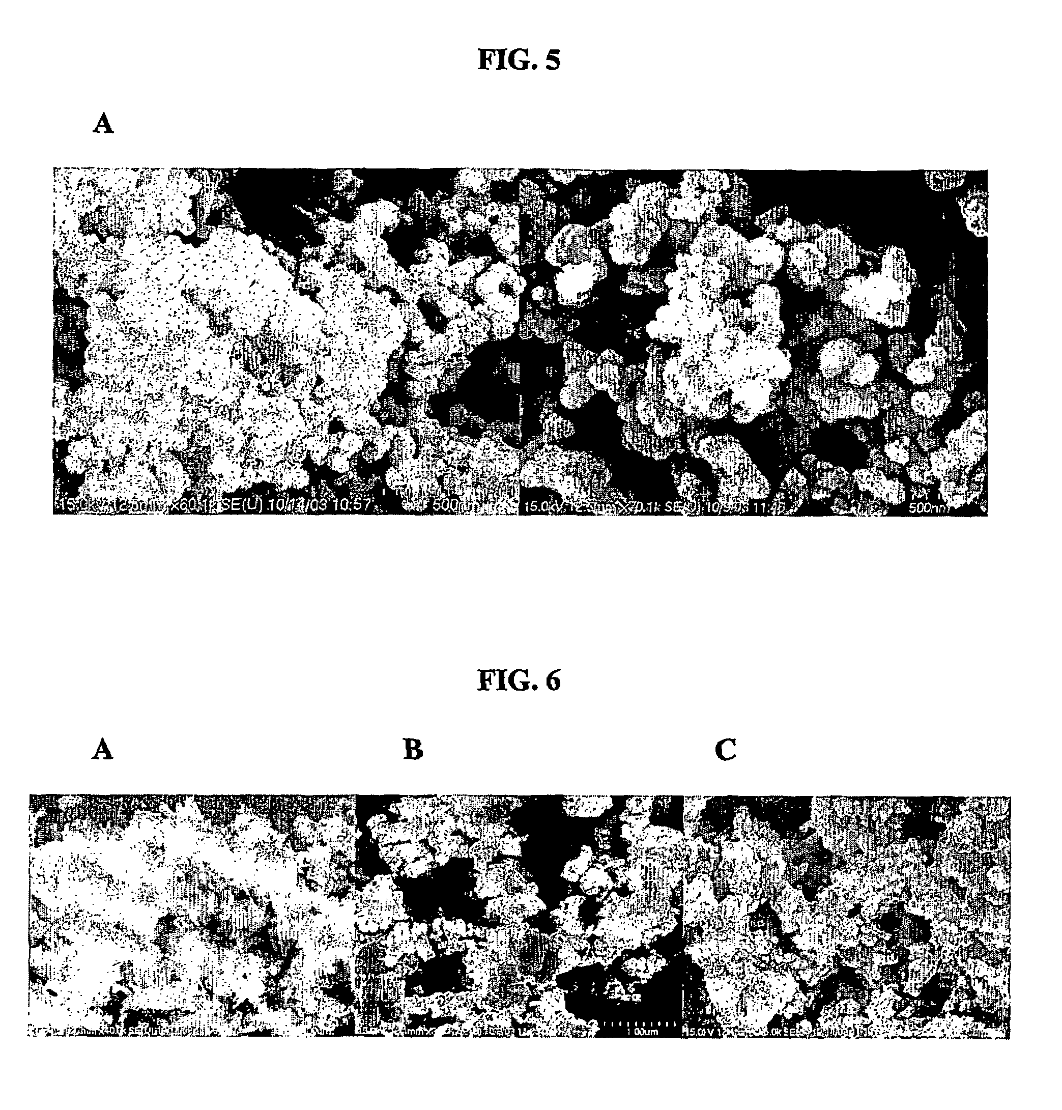
[0063]The preparation method of NdS2 nanoparticles from Nd2O3 nanoparticles was applied to other rare-earth oxide nanoparticles with success. The products were all fine powders of the pure sulfides after sulfidation reactions at the temperature range between 350 and 550° C. The scanning electron microscopic (SEM) images of the products showed that the particle sizes varied significantly from 30 nm to ˜1 μm, and the sizes were smaller when the reaction temperature was lower. FIGS. 5-9 show the SEM images of the various nanoparticles. FIG. 5 lows nanoparticles of TbS2 (IA) from Tb4O7 nanoparticles (FIG. 5; average size=45-60 nm in diameter). The loaded molar ratio was Tb4O7:B:S=3:14:24. The preparation was heated at 450° C. for 24 hours. FIG. 6 shows nanoparticles of starting material Ce2O3 (FIG. 6A; avera...

example 3

Synthesis of Metal Polysulfides and Sulfides (TiS2, TiS3, VS4, FeS2, NiS2, NbS3, MoS2, RuS2, WS2, Y2S3, RS2 (R═Ce, Nd, Sm, Eu, Th and Er), In2S3, PbS, PbTe, BaTiS3, KInS2, NaInS2, NaInSe2, NaBiS2) from their Binary and / or Ternary Oxides at Intermediate Temperatures

[0065]Amorphous boron powder (99.99%, 325 mesh), sulfur powder (99.999%) and metal oxides (99.9% or higher) were purchased from Alfa Aesar. The reaction materials in the scale of mmol were loaded in a glove box or in air. In a general reaction scheme, a metal oxide in powder was placed in a short fused silica tube (FIG. 1). Stoichiometric amounts of boron and sulfur powders were mixed and placed in a separate fused silica tube of the same size. The reactant ratios were chosen to provide the most sulfur-rich phases in the phase diagrams at the designated reaction temperatures. To ensure a complete reaction of metal oxides, sulfur was loaded 10% more than the stoichiometric amounts. The two tubes were subsequently situated i...


PUM

PropertyMeasurementUnit
melting pointaaaaaaaaaa
temperatureaaaaaaaaaa
diameteraaaaaaaaaa

Abstract

A method of preparing metal chalcogenides from elemental metal or metal compounds has the following steps: providing at least one elemental metal or metal compound; providing at least one element from periodic table groups 13-15; providing at least one chalcogen; and combining and heating the chalcogen, the group 13-15 element and the metal at sufficient time and temperature to form a metal chalcogenide. A method of functionalizing the surface of semiconducting nanoparticles has the following steps: providing at least one metad compound; providing one chalcogenide having a cation selected from the group 13-15 (B, Al, Ga, In, Si, Ge, Sn, Pb, P, As, Sb and Bi); dissolving the chalcogenide in a first solution; dissolving the metal compound in a second solution; providing and dissolving a functional capping agent in at least one of the solutions of the metal compounds and chalcogenide; combining all solutions; and maintaining the combined solution at a proper temperature for an appropriate time.

Description

CROSS-REFERENCE TO RELATED APPLICATIONS[0001]This application claims benefit to U.S. provisional application Ser. Nos. 60 / 444,078 and 60 / 511,482, filed on Jan. 31, 2003 and Oct. 15, 2003, respectively, and International Application Number PCT / US504 / 02929 filed on Feb. 2, 2004.TECHNICAL FIELD[0002]The present invention relates to methods of synthesis of metal chalcogenides from metal compounds and period table group 13-15 elements combined with a chalcogen.BACKGROUND ART[0003]Because of their wide range of physical and chemical properties and unique structural characteristics, chalcogenides (sulfides, selenides and tellurides) of metals are widely used in industrial applications such as catalysis, lubrications, battery fabrication, ionic conduction, refractories, pigments, sensors, and optical and magnetic devices. Among the various preparation methods of metal chalcogenides, the simplest method to date is based on direct reactions between chalcogen elements and elemental metals at e...

Claims


Application Information

Patent Timeline
Patent Type & Authority Patents(United States)
IPC IPC(8): C01B17/00C01B19/00C01G1/00C01B17/20C01F17/00C01G1/12C09K11/56C09K11/88H01M4/02H01M4/58
CPCB82Y30/00C01B19/007C01F17/0087C01G1/00C01G1/12C01G35/00C01G39/06C01G41/00C01G49/12C01G55/00C09K11/565C09K11/883H01M4/58H01M4/581H01M4/5815C01B17/20Y10S977/777C01P2002/72C01P2002/77C01P2002/78C01P2002/84C01P2004/03C01P2004/04C01P2004/16C01P2004/20C01P2004/64C01P2006/60H01M2004/028Y10S977/773Y10S977/762Y10S977/775C01F17/288Y02E60/10
Inventor SEO, DONG-KYUNIANCU, NORAWU, LIMING
Owner ARIZONA STATE UNIVERSITY
Why Eureka
Try Eureka