Wave transmission medium and waveguide circuit

a waveguide circuit and transmission medium technology, applied in the field of wave transmission medium and waveguide circuit, can solve the problems of reducing the flexibility of circuit configuration, sharply increasing the size of optical circuit, and increasing the optical path length of optical waveguide circuit, so as to achieve high efficiency, compact optical circuit, and flexible optical input/output.

Active Publication Date: 2008-07-08
NIPPON TELEGRAPH & TELEPHONE CORP
View PDF14 Cites 23 Cited by
  • Summary
  • Abstract
  • Description
  • Claims
  • Application Information

AI Technical Summary

Benefits of technology

[0015]The present invention is implemented to solve the foregoing problems. An object of the present invention is to provide an optical (wave) transmission medium for implementing an optical circuit that is smaller in size than an optical circuit using the conventional optical waveguide circuit or plane holographic circuit, that can arrange the input / output of light as flexibly as possible, and that enables sufficiently highly efficient optical signal control even with mild refractive index distribution (with small undulations), thereby implementing a highly efficient, compact waveguide circuit, and providing an arrayed waveguide grating type optical multi / demultiplexing circuit with small chromatic dispersion.
[0073]According to the present invention, the optical (wave) transmission medium is provided that is smaller in size than the conventional optical circuit using the optical waveguide circuit or plane holographic circuit; that can set up the optical input / output as flexibly as possible; and that implements a waveguide circuit enabling highly efficient optical signal control even with a mild refractive index distribution (small undulations of the refractive index difference). Thus, it can implement a highly efficient, compact optical circuit.
[0074]In addition, the arrayed waveguide type optical multi / demultiplexer in accordance with the present invention has a plurality of scattering points placed in the input waveguide in accordance with the spatial refractive index distribution. Thus, it controls the phase and intensity of the propagation light simultaneously, thereby being able to provide a low dispersion arrayed waveguide type optical multi / demultiplexer that can reduce the chromatic dispersion.

Problems solved by technology

Consequently, it is inevitable that optical path length of the optical waveguide circuit becomes longer than the optical path length required for bringing about interference in the optical circuit.
This presents a problem of sharply increasing the size of the optical circuit.
The optical confinement utilizing such a large refractive index difference presents a problem of reducing the flexibility of a circuit configuration.
Thus, the optical circuit inevitably becomes long, which makes it difficult to miniaturize the optical circuit.
Consequently, the optical circuit has a substantially uniform structure for a wavefront, thereby making it difficult to control the light in the direction perpendicular to the propagation direction (in the direction of the wavefront).
In addition, as for a circuit that varies a spot position sharply in a direction perpendicular to the propagation direction, such as a branching circuit, since the optical field must be greatly expanded in the direction perpendicular to the propagation direction, the size of the circuit inevitably becomes large.
Thus, the design is limited to a circuit with a strictly periodic structure (that is, an optical circuit depending on the wave number in the propagation direction).
This increases the circuit scale, makes the circuit sensitive to the wavelength, and has the input / output positions distributed sequentially in accordance with the wavelengths, thereby presenting a problem of limiting the design to circuits with little flexibility.
Since the chromatic dispersion provides different delay times to signal spectral components, the conventional extended-passband arrayed waveguide grating type optical multi / demultiplexing circuit with the large chromatic dispersion has a problem of bringing about considerable optical pulse degradation.

Method used


Image

  • Wave transmission medium and waveguide circuit
  • Wave transmission medium and waveguide circuit
  • Wave transmission medium and waveguide circuit

Examples


embodiment 1

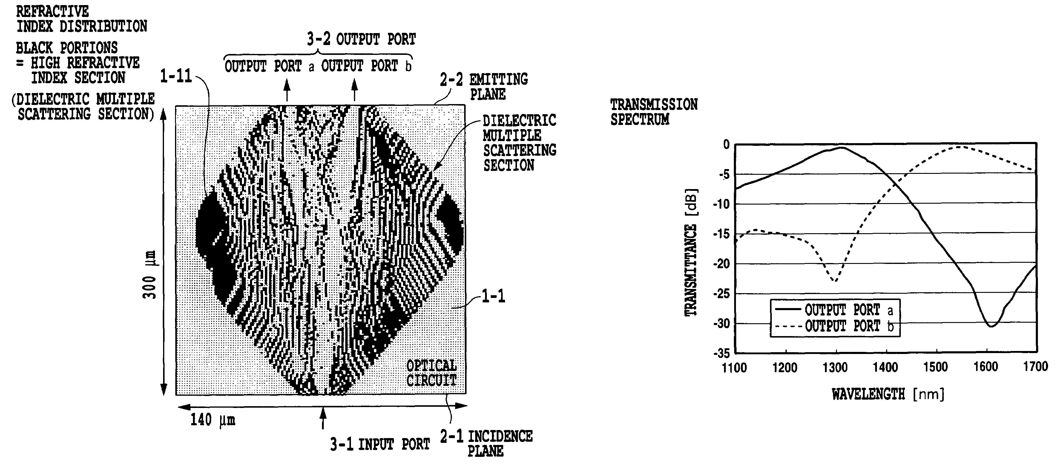
[0221]As for the so-called step-index optical circuit, it is not self-evident as to whether an optical circuit can be designed according to the foregoing expression (1) because the value the refractive index can take is limited. However, even in the case where the value the refractive index can take is limited, it is possible to adjust the optical phase globally by repeating adjustment of the local refractive indices. Therefore it is possible to design the optical circuit by assuming a steplike refractive index distribution that has an upper limit of the refractive index of the dielectric constituting the optical circuit and a finite number of refractive indices reaching the upper limit, and by calculating the refractive index distribution of the optical circuit using the refractive indices as a limit value. The present embodiment designs the optical circuit based on such an idea.

[0222]In the present embodiment, the idea is applied to an optical waveguide that has the same structure...

embodiment 2

[0237]The present embodiment designs the same optical circuit as that of the embodiment 1 in accordance with the following calculation method of the refractive index distribution. The outline of the optical circuit will be briefly described with reference to FIG. 5, again. First, an arbitrary refractive index distribution {n} is given, and the field distribution 1, ψj(z, x, {n}), of the input light corresponding to the distribution {n} is calculated. Then, the reverse propagation light (field distribution 2, fj(z, x, {n})) with the field expected to be output from the output port as the output light is successively calculated by virtually transmitting the reverse propagation light toward the incidence plane 2-1.

[0238]Take an example of FIG. 8. First, the refractive index distribution is changed such that the phase of the cross section ψj(zx, x, {n}) of the field distribution 1 at a location z=zx matches the phase of the cross section fj(zx+Δz, x, {n}) of the field distribution 2 at ...

embodiment 3

[0257]In the present embodiment, a design method will be described of a wavelength division multi / demultiplexing circuit for demultiplexing and / or multiplexing four wavelengths 1.53 μm, 1.54 μm, 1.55 μm and 1.56 μm.

[0258]FIGS. 16A and 16B are diagrams illustrating condition settings for the optical circuit design of the four-wavelength demultiplexer of the present embodiment: FIG. 16A illustrates the case where only a TE mode is set as the polarization state of the input light; and FIG. 16B illustrates the case where a TM mode in addition to the TE mode is set as the polarization state of the input light.

[0259]First, in the case of setting only the TE mode, wavelength division multiplexed light is input to the input port 3-1, and optical waves with different wavelengths are emitted from the individual ports of the output port 3-2 as illustrated in FIG. 16A. The incidence plane 2-1 includes one input port 3-1, and the emitting plane 2-2 includes four ports a, b, c and d. The light in...


PUM


Abstract

A wave transmission medium includes an input port 3-1 and an output port 3-2. A field distribution 1 and a field distribution 2 are obtained by numerical calculations. The field distribution 1 is a field distribution of the propagation light (forward propagation light) launched into the input port 3-1. The field distribution 2 is a field distribution of the phase conjugate light (reverse propagation light) resulting from reversely transmitting from the output port side an output field that is expected to be output from the output port 3-2 when an optical signal is launched into the input port 3-1. According to the field distributions 1 and 2, a spatial refractive index distribution is calculated such that the phase difference between the propagation light and reverse propagation light is eliminated at individual points (x, z) in the medium.

Description

TECHNICAL FIELD[0001]The present invention relates to a wave transmission medium and a waveguide circuit using it, and a fabrication method thereof, and more particularly to a medium for transmitting waves using multiple scattering in accordance with two-dimensional refractive index distribution and a waveguide circuit configured using it, and to a fabrication method thereof.BACKGROUND ART[0002]In a technical field such as optical communication, integrated optical components utilizing an optical waveguide structure have been developed to construct optical circuits for easily implementing optical splitting and interference. The integrated optical components utilizing the property of waves make it to adjust optical path length and to facilitate fabrication of interferometers. In addition, applying the semiconductor circuit processing technique enables integration of optical components.[0003]However, since these optical waveguide circuits construct individual components of optical circ...

Claims


Application Information

Patent Timeline
Patent Type & Authority Patents(United States)
IPC IPC(8): G02B6/12G02B6/34
CPCG02B6/12009G02B6/12007G02B5/32G02B6/12014G02B6/12016G02B6/125G02B2006/1215
Inventor HASHIMOTO, TOSHIKAZUOGAWA, IKUOKITAGAWA, TAKESHISUZUKI, SENICHIYANAGISAWA, MASAHIROSHIBATA, TOMOHIROKOUTOKU, MASAKITAKAHASHI, HIROSHINAGASE, RYOUKOBAYASHI, MASARUASAKAWA, SHUICHIROABE, YOSHITERUKITOH, TSUTOMUOHYAMA, TAKAHARU
Owner NIPPON TELEGRAPH & TELEPHONE CORP
Why Eureka
Try Eureka