

Non-thermal process for forming porous low dielectric constant films
a low dielectric constant, non-thermal technology, applied in the direction of electric/magnetic/electromagnetic heating, nuclear engineering, transportation and packaging, etc., can solve the problems of ic devices such as cu metal lines that cannot be subjected to processing temperatures for short time periods, and their performance deteriorates, and damage the resultant film
- Summary
- Abstract
- Description
- Claims
- Application Information
AI Technical Summary
Problems solved by technology
Method used
Image

Examples
examples
[0075]The sample films were formed via a plasma enhanced CVD process using an Applied Materials Precision-5000 system in a 200 mm DxZ vacuum chamber that was fitted with an Advance Energy 200 rf generator and using an undoped TEOS process kit. The CVD process involved the following basic steps: initial set-up and stabilization of gas flows deposition, and purge / evacuation of chamber prior to wafer removal.
[0076]The thickness and refractive index of each film were measured on an SCI Filmtek 2000 Reflectometer. Dielectric constants were determined using Hg probe technique on low resistivity p-type wafers (<0.02 ohm-cm). Mechanical properties were determined using MTS Nano Indenter.
[0077]In some of the following examples, UV exposure was performed using a Fusion UV model F305 ultraviolet lamp. The films subjected to UV exposure were placed in a 2″ diameter quartz glass tube with sealed end caps. In examples involving a vacuum or inert atmospheres, three pump and purge cycles were perfo...
example 1
DEMS Film Having ATP as Pore-Former Subjected to UV Exposure
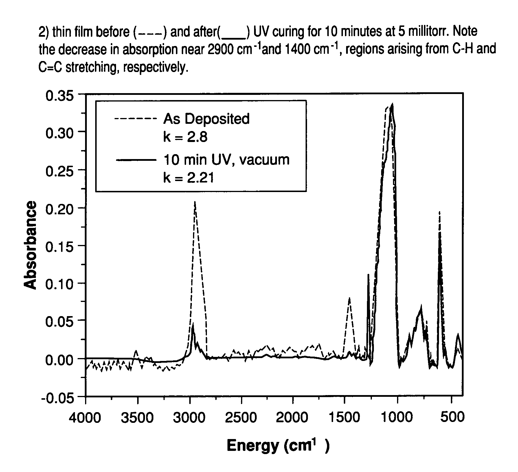
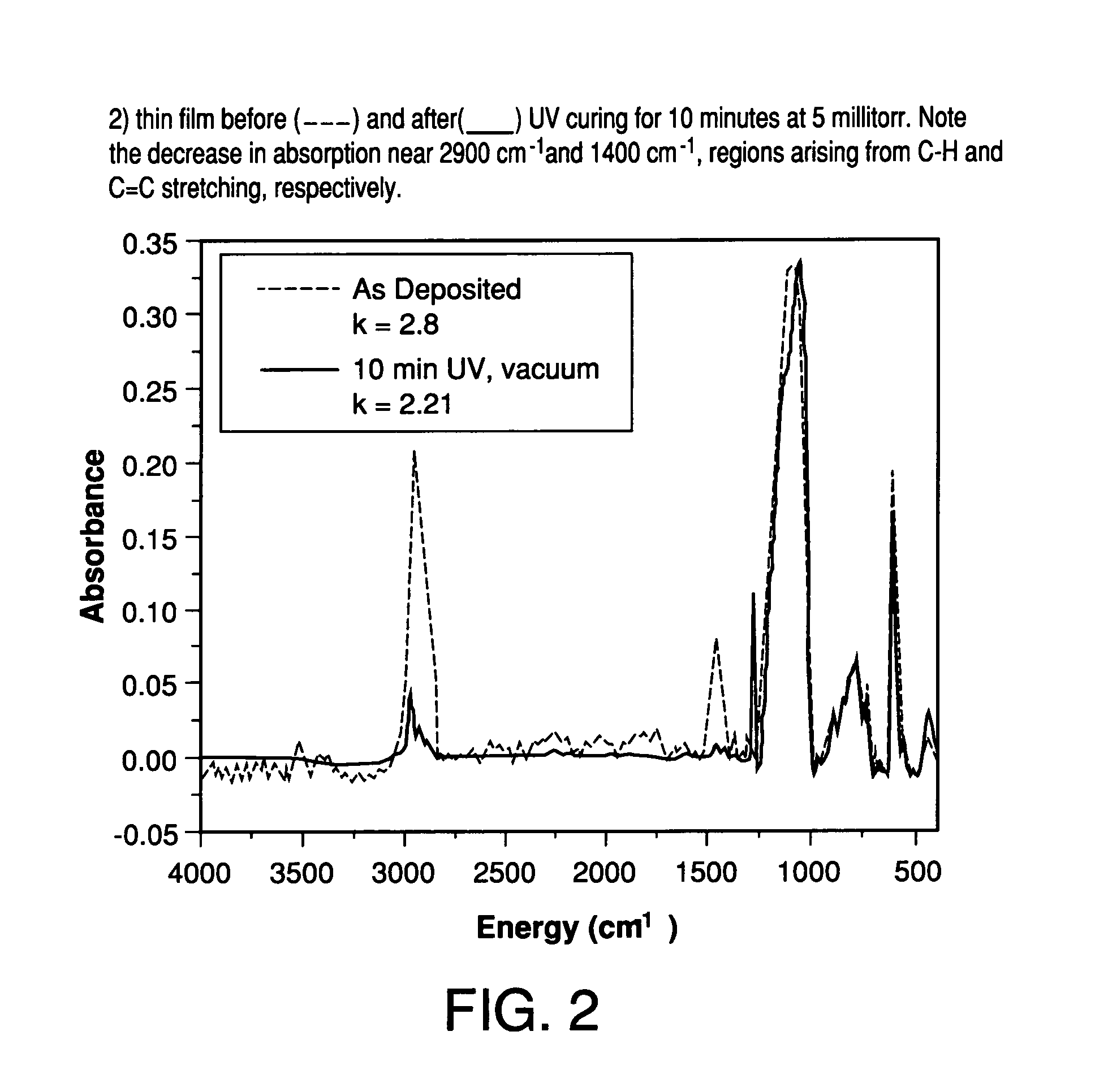
[0079]A multiphasic film formed via plasma enhanced chemical vapor codeposition (PECVD) of diethoxy methylsilane as the structure-forming phase and ATP as the pore-forming phase and carbon dioxide as carrier gas had the following properties before UV exposure: thickness of 1018 nm, dielectric constant of 2.8, and refractive index of 1.509. The film was exposed to UV light at a pressure of 5 millitorr for 10 minutes. The temperature of the film reached approximately 200° C. during the exposure. The thickness after UV exposure was 790 nm, and the refractive index was 1.363. The dielectric constant was 2.21.
[0080]FIG. 2 displays an infrared spectra of the film before (see dashed line) and after (see solid line) UV exposure, indicating reduced absorption in the C—H and C═C regions of the spectrum following UV exposure. The reduced absorption in these regions of the spectrum may indicate that the pore-forming phase, or ATP, is s...
example 2
DEMS Film Having ATP as Pore-Former Subjected to UV Exposure and Post-UV Exposure Thermal Treatment
[0082]A multiphasic film formed via plasma enhanced chemical vapor codeposition (PECVD) of diethoxy methylsilane as the structure-forming phase and ATP as the pore-forming phase and carbon dioxide as carrier gas had the following properties before UV exposure: thickness of 1008 nm, a dielectric constant of 2.8, and a refractive index of 1.504. The film was exposed to UV light at a pressure of 5 millitorr for 10 minutes. The temperature of the film reached approximately 200° C. during the curing process. The thickness after curing was 847 nm, and the refractive index was 1.369. The dielectric constant was 2.25. The film was then heated in a tube furnace to 425° C. for 90 minutes at ambient pressure under nitrogen purge. The thickness after thermal curing was 800 nm, and the refractive index was 1.359. The dielectric constant was 2.24. The film properties before and after thermal treatme...
PUM
| Property | Measurement | Unit |
|---|---|---|
| dielectric constant | aaaaa | aaaaa |
| wavelengths | aaaaa | aaaaa |
| wavelengths | aaaaa | aaaaa |
Abstract
Description
Claims
Application Information