Integrator circuitry for single channel radiation detector

Inactive Publication Date: 2008-08-12
NASA
View PDF26 Cites 43 Cited by
  • Summary
  • Abstract
  • Description
  • Claims
  • Application Information

AI Technical Summary

Benefits of technology

[0038]A possible advantage of the present invention may comprise utilizing sufficient bits in an analog to digital circuit for processing the detected peak voltage to provide a wide dynamic range over which the detected peak voltage can be usefully processed thereby eliminating electronic design adjustments for particular detectors and/or the ability to process high and low energy pulses in a single electronics channel.
[0039]Yet another possible objective of the present invention may comprise producing data collection processing signals locally without the need for a central computer.
[0040]Yet another possible objective of the present invention may comprise features of the circuitry which may be reprogrammed either remotely or locally.
[0041]Yet another possible objective of the present invention may comprise a radiation detector circuit that may be utilized with a variety of different radiation detectors.
[0042]Any listed objects, features, and advantages are not intended to limit the invention or claims in any conceivable manner but are intended merely to be informative of some of the objects, features, and advantages of the present invention. In fact, these and yet other objects, features, and advantages of the present invention will become apparent from the drawings, the descriptions given herein, and the appended claims.
[0043]Accordin

Problems solved by technology

The two channel radiation detection circuits require two separate circuits with different gains and threshold settings thereby requiring significant cost and reducing reliability.
Therefore related art radiation detector circuitry is limited in flexibility of use with different radiation detectors.
Related art radiation detector circuitry are limited in various ways such as the two channel configuration and in other ways as discussed hereinafter that hinder or prevent this function.
Related art circuitry for multiple radiation detector systems not only tend to produce less accurate data, and require the more bulky two channel layout, but are also likely to miss data such as coincident detection o

Method used


Image

  • Integrator circuitry for single channel radiation detector
  • Integrator circuitry for single channel radiation detector
  • Integrator circuitry for single channel radiation detector

Examples


Embodiment Construction

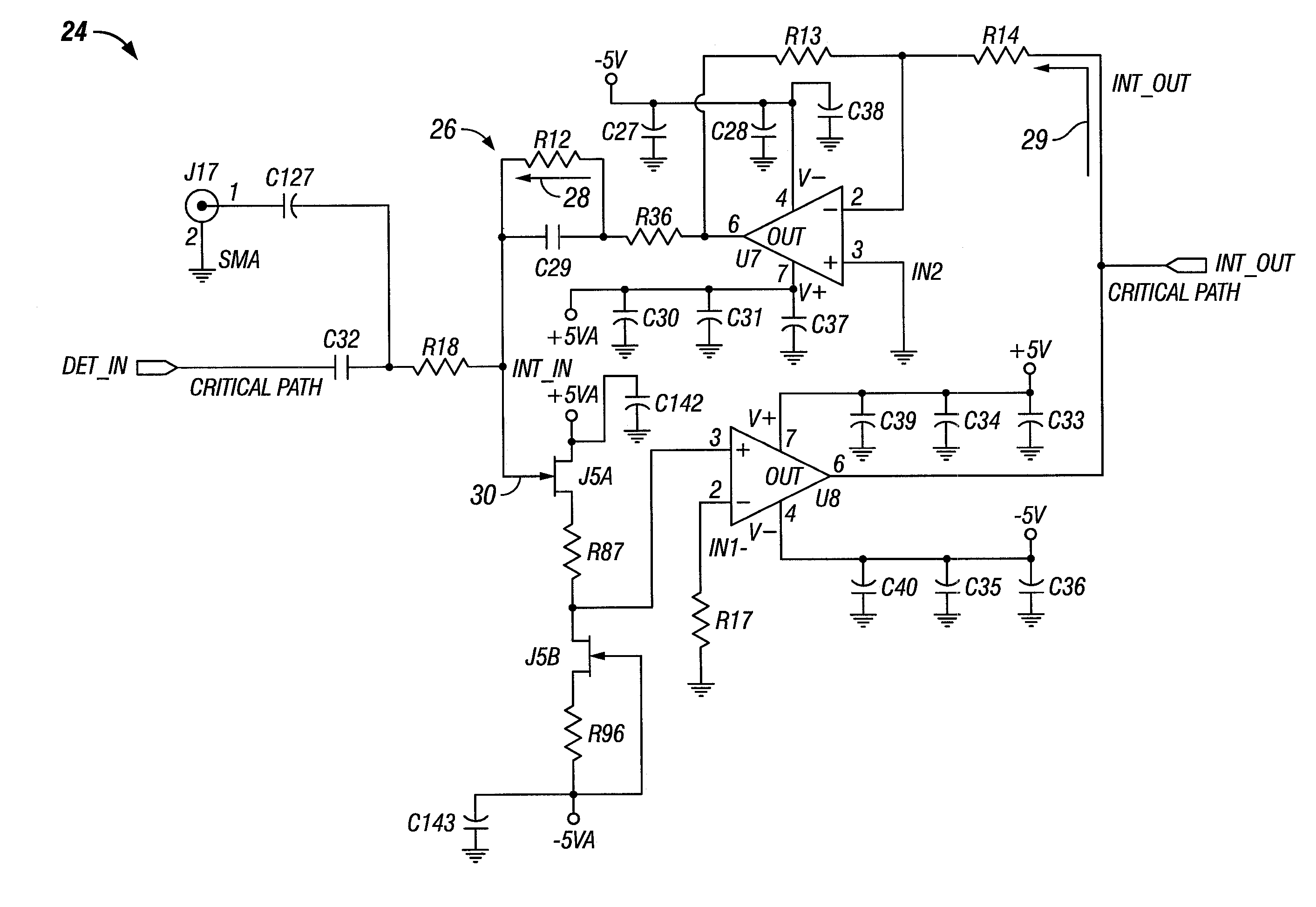
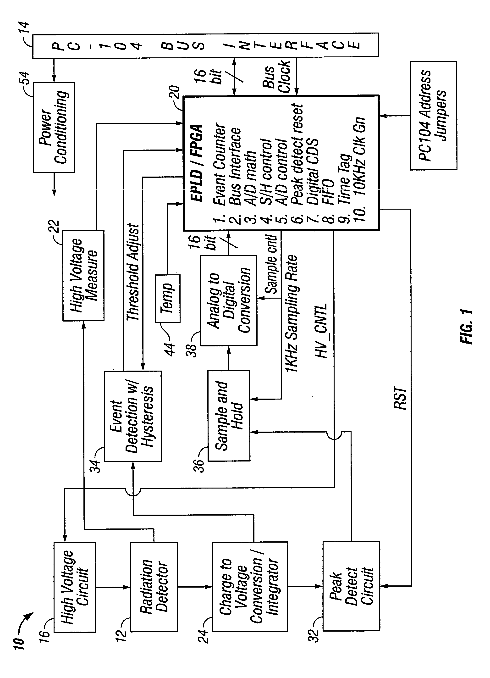
[0086]Referring now to the drawings, and more particularly to FIG. 1, there is shown a block diagram for radiation detector circuit 10 in accord with one possible embodiment of the present invention. Radiation detector circuit 10 is programmable to operate with different radiation detectors and in a manner that is believed to improve operation of related art radiation circuits. Accordingly, radiation detector circuit 10 interfaces to radiation detector 12 and provides radiation events data to data bus 14 which may be a PC104 computer bus interface or other computer bus. Multiple radiation detector circuits 10 can be stacked together in a PC104, or other computer bus, bus stack to create a multiple detector system as indicated in FIG. 11.

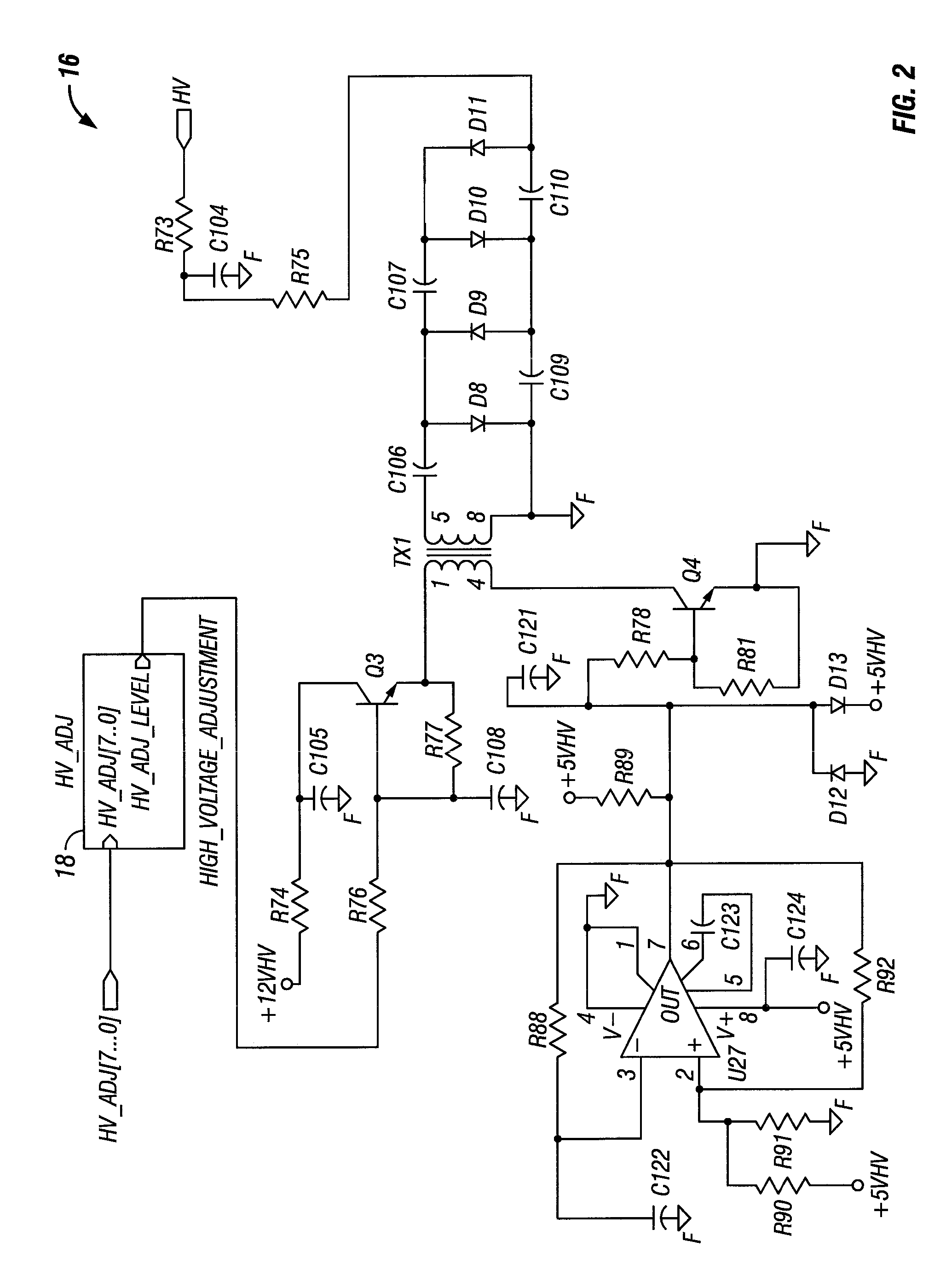
[0087]Radiation detector circuit 10 may be programmed to operate with a wide range of different types of radiation detectors 12 by providing the high voltage and interfacing to detect the signal produced thereby. In one embodiment, the radiation dete...


PUM


Abstract

Input circuitry is provided for a high voltage operated radiation detector to receive pulses from the detector having a rise time in the range of from about one nanosecond to about ten nanoseconds. An integrator circuit, which utilizes current feedback, receives the incoming charge from the radiation detector and creates voltage by integrating across a small capacitor. The integrator utilizes an amplifier which closely follows the voltage across the capacitor to produce an integrator output pulse with a peak value which may be used to determine the energy which produced the pulse. The pulse width of the output is stretched to approximately 50 to 300 nanoseconds for use by subsequent circuits which may then use amplifiers with lower slew rates.

Description

ORIGIN OF THE INVENTION[0001]The invention described herein was made by employee(s) of the United States Government and may be manufactured and used by or for the Government of the United States of America for governmental purposes without the payment of any royalties thereon or therefore.BACKGROUND OF THE INVENTION[0002]1. Field of the Invention[0003]The present invention relates generally to radiation detectors and, more particularly, to integrator circuitry and circuitry related thereto for providing a single channel circuit for a radiation detector.[0004]2. Description of Related Art[0005]Electronic circuits for radiation detectors have been utilized for over a century for the purpose of detecting pulses produced in a radiation sensor element as a result of impingement by some type of radiation. Presently, two channel radiation detection circuits are commonly utilized when it is desired to detect high energy and low energy pulses from the same radiation detector. The two channel...

Claims


Application Information

Patent Timeline
IPC IPC(8): G01T1/24G06G7/12
CPCG06G7/18
Inventor HOLLAND, SAMUEL D.DELAUNE, PAUL B.TURNER, KATHRYN M.
Owner NASA
Why Eureka
Try Eureka