

Spin-polarized electron source and spin-polarized scanning tunneling microscope
a scanning tunneling microscope and spin-polarized electron technology, applied in the field of spintronics, can solve the problems that the conventional spin-polarized electron source, as mentioned above, would not meet the requiremen
- Summary
- Abstract
- Description
- Claims
- Application Information
AI Technical Summary
Benefits of technology
Problems solved by technology
Method used
Image

Examples
Embodiment Construction
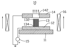
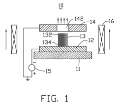
[0019]Referring to FIG. 1, a spin-polarized electron source 10, in accordance with a first preferred embodiment, is provided. The spin-polarized electron source 10 can realize continuous and efficient emission of a spin-polarized electron current / beam under an effect of a magnetic field induction. Specifically, the spin-polarized electron source 10 includes: a glass substrate 11, a cathode 12, one-dimensional (i.e., one dimension predominating) nanostructures 13 of group III-V compound semiconductors with local occupied polarized gap states (i.e., polarized gap states being occupied by electrons and being localized), an anode 14, and a magnetic field generator 16.
[0020]The cathode 12 is disposed on the glass substrate 11. The cathode 12 is suitably made from an electrically conductive material, including, for example, a tin indium oxide, a n-type doped silicon, or a p-type doped silicon.
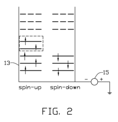
[0021]The one-dimensional nanostructures 13 made of at least one group III-V compound semiconduct...
PUM
| Property | Measurement | Unit |
|---|---|---|
| thick | aaaaa | aaaaa |
| Curie temperature | aaaaa | aaaaa |
| aspect ratio | aaaaa | aaaaa |
Abstract
Description
Claims
Application Information