Method for fabricating metal-oxide semiconductor transistors

a technology of metal-oxide semiconductors and transistors, which is applied in the direction of transistors, basic electric elements, electric devices, etc., can solve the problems of poor threshold voltage roll-off characteristic, formation hits a limitation, and the implantation process also creates significant interstitial defects, and achieves enhanced diffusion

Active Publication Date: 2009-01-06
UNITED MICROELECTRONICS CORP
View PDF6 Cites 27 Cited by
  • Summary
  • Abstract
  • Description
  • Claims
  • Application Information

AI Technical Summary

Benefits of technology

[0013]The present invention specifically implants a molecular cluster containing boron into the semiconductor substrate for forming an ultra-shallow junction while eliminating the needs of performing any pre-amorphorized implantation. According to the preferred embodiment of the present invention, the implanted molecular cluster is preferably composed of molecules having large molecular weight, such as B10H14 or B18H22, in which the weight ratio of each boron atom within the molecular cluster is preferably less than 10%. Thereafter, a millisecond annealing process can be conducted to activate the implanted molecular cluster. By eliminating the needs of conducting any pre-amorphorized implantation process while forming ultra-shallow junctions, the present invention is able to prevent various drawbacks caused by the pre-amorphorized implantation process, including interstitial defects generated by the impact of dopants injected into the lattice structure of the silicon substrate, transient enhanced diffusion caused by rapid boron diffusion during a rapid thermal annealing process, or end of range dislocation phenomenon.

Problems solved by technology

However, a short channel effect, which results in a poor threshold voltage roll-off characteristic, always accompanies miniaturization.
However, as device scale is reduced to 90-nm and smaller, the conventional ultra shallow junction formation hits a limitation in depth control, and co-implantation performed in cooperation with pre-amorphorization (PAI) and laser annealing seems to be able to satisfy demands down to 65-nm and even 45-nm processes.
It should be noted that despite the fact that the conventional pre-amorphorized implantation process can be conducted to achieve ultra-shallow junctions by injecting non-doping ions for inhibiting the diffusion of dopants implanted thereafter, the implantation process also creates significant interstitial defects while using the implanted ions to damage the lattice structure of the silicon substrate.
This transient enhanced diffusion effect not only deepens the junction profile but also makes the distribution of the dopant not sheer in the lateral direction, resulting in an end of range dislocation phenomenon and a severe short channel effect.

Method used


Image

  • Method for fabricating metal-oxide semiconductor transistors
  • Method for fabricating metal-oxide semiconductor transistors
  • Method for fabricating metal-oxide semiconductor transistors

Examples


Embodiment Construction

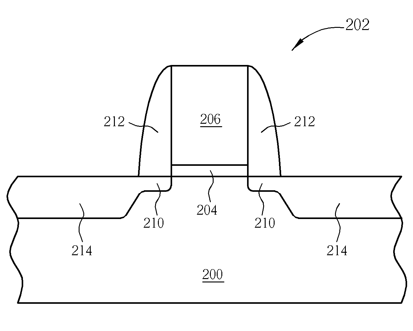
[0019]Please refer to FIGS. 4-6. FIGS. 4-6 illustrate a method for fabricating a PMOS transistor according to the preferred embodiment of the present invention. As shown in FIG. 4, a semiconductor substrate 200 having a gate structure 202 thereon is provided, in which the semiconductor substrate 200 can be a semiconductor wafer or a silicon on insulator substrate. The gate structure 202 includes a gate dielectric 204 and a gate 206 disposed on the gate dielectric 204. The gate dielectric 204 is preferably composed of insulating materials such as silicon dioxide and the gate 206 is composed of conductive materials such as doped polysilicon.

[0020]As shown in FIG. 5, an ion implantation process is performed by injecting large molecular ions or clustered ions having p-type dopants into the semiconductor substrate 200 surrounding the gate structure 204 to form a lightly doped drain 210. Preferably, the molecular ions can be a molecular cluster having boron therein. According to the prefe...


PUM


Abstract

A method for fabricating a metal-oxide semiconductor transistor is disclosed. First, a semiconductor substrate having a gate structure thereon is provided, and a spacer is formed around the gate structure. An ion implantation process is performed to implant a molecular cluster containing boron into the semiconductor substrate surrounding the spacer for forming a source / drain region. The weight ratio of each boron atom within the molecular cluster is preferably less than 10%. Thereafter, a millisecond annealing process is performed to activate the molecular cluster within the source / drain region.

Description

CROSS REFERENCE TO RELATED APPLICATIONS[0001]This application claims the benefit of the filing date of U.S. provisional patent application No. 60 / 766,954 (filed Feb. 22, 2006), the contents of which are hereby incorporated by reference.BACKGROUND OF THE INVENTION[0002]1. Field of the Invention[0003]The invention relates to a method for fabrication metal-oxide semiconductor transistors.[0004]2. Description of the Prior Art[0005]With progress in the semiconductor industry, performance and economic factors of integrated circuit design and manufacture have caused a scale of devices in integrated circuits to be drastically reduced to miniaturized sizes, increasing density on a chip. However, a short channel effect, which results in a poor threshold voltage roll-off characteristic, always accompanies miniaturization. To avoid this problem, industries have provided a method for forming lightly doped drains (LDDs) having an ultra shallow junction as a solution.[0006]In a conventional ultra ...

Claims


Application Information

Patent Timeline
Patent Type & Authority Patents(United States)
IPC IPC(8): H01L21/336H01L21/42H01L21/425
CPCH01L21/265H01L21/2652H01L21/324H01L29/6659H01L21/26566H01L21/2658
Inventor HSIAO, TSAI-FULI, CHING-ICHEN, PO-YUANLIN, CHUN-ANWANG, HSIANG-YINGCHEN, CHAO-CHUNCHIEN, CHIN-CHENG
Owner UNITED MICROELECTRONICS CORP
Why Eureka
Try Eureka