Low temperature aerosol deposition of a plasma resistive layer

a plasma resistive layer and low temperature technology, applied in the field of semiconductor processing, can solve the problems of poor uniformity of the coated layer, reduced chamber component life, and surface cracks

Active Publication Date: 2009-01-20
APPLIED MATERIALS INC
View PDF12 Cites 50 Cited by
  • Summary
  • Abstract
  • Description
  • Claims
  • Application Information

AI Technical Summary

Problems solved by technology

Attack from corrosive species also reduces the lifespan of the chamber components.
Additionally, flakes of the eroded parts of the chamber component may become a source of particulate contamination during substrate processing.
However, high temperature processing may deteriorate surface properties or adversely modify the microstructure of the coated surface, resulting in a coated layer having poor uniformity and / or surface cracks due to temperature elevation.
Furthermore, if the coated layer or the underlying surface has microcracks or the coatings are not applied uniformly, the component surface may deteriorate over time and eventually expose the underlying component surface to corrosive plasma attack.

Method used


Image

  • Low temperature aerosol deposition of a plasma resistive layer
  • Low temperature aerosol deposition of a plasma resistive layer
  • Low temperature aerosol deposition of a plasma resistive layer

Examples


Embodiment Construction

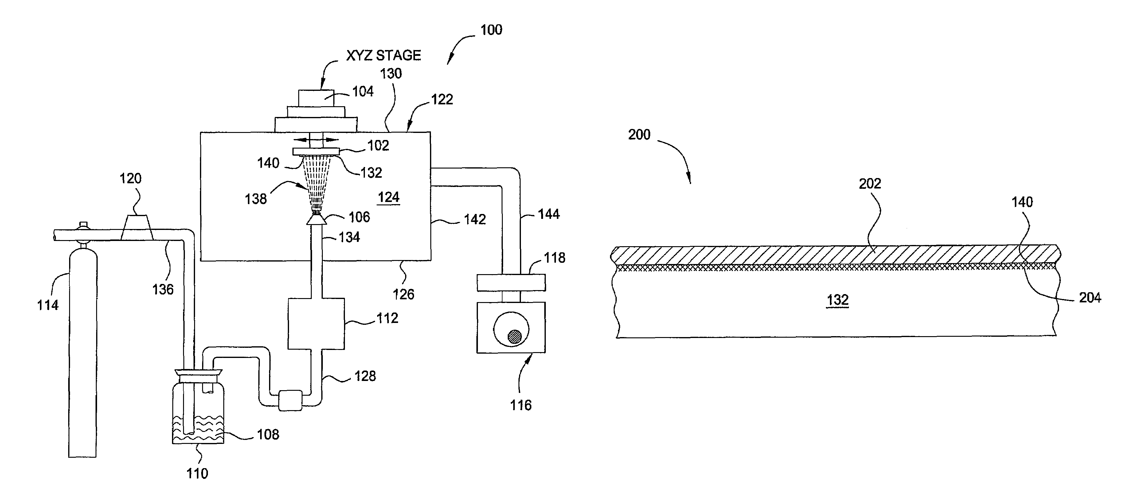
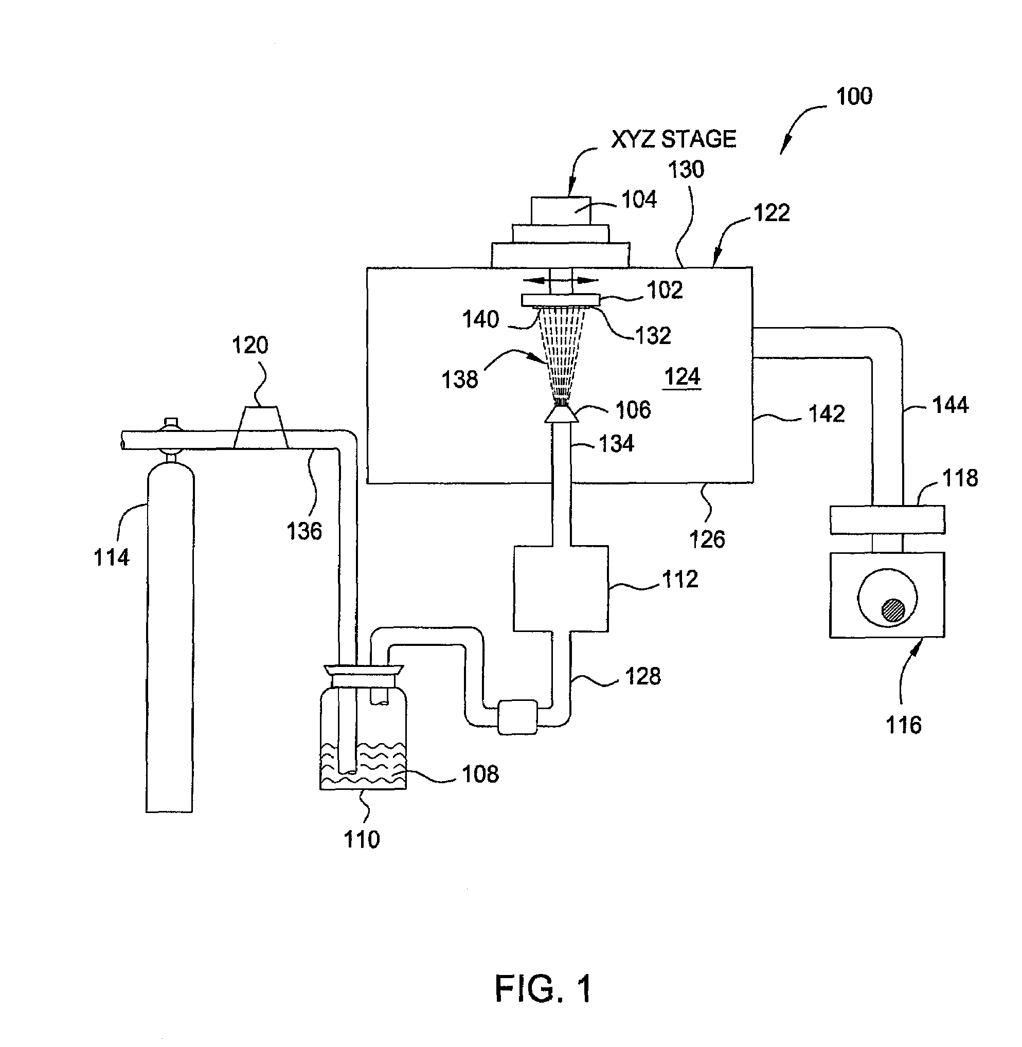
[0016]FIG. 1 is a sectional view of one embodiment of an apparatus 100 that may be utilized to perform an aerosol deposition (AD) process according to the present invention. The inventive aerosol deposition (AD) process forms a plasma resistive layer that may be utilized to beneficially protect surfaces exposed to plasma process. The apparatus 100 includes a processing chamber 122 having a top 130, a bottom 126, and sidewalls 142 that define a process region 124 in the interior volume of the processing chamber 122. A stage 104 is disposed on the top 130 of the processing chamber 122 to a substrate holder 102 that holds a substrate 132 during processing. The stage 104 is configured to move the holder 102 along the X, Y, and Z axes. Thus, the stage 104 moves the substrate 132 positioned thereon along the X, Y, and Z axis. A mechanical booster pump 116 and a rotary pump 118 are coupled to the processing region 124 through a port formed in the sidewall 142 of the processing chamber 122 ...


PUM

PropertyMeasurementUnit
temperatureaaaaaaaaaa
diameteraaaaaaaaaa

Abstract

Embodiments of the present invention provide a method for low temperature aerosol deposition of a plasma resistive layer on semiconductor chamber components / parts. In one embodiment, the method for low temperature aerosol deposition includes forming an aerosol of fine particles in an aerosol generator, dispensing the aerosol from the aerosol generator into a processing chamber toward a surface of a substrate, maintaining the substrate temperature at between about 0 degrees Celsius and 50 degrees Celsius, and depositing a layer from material in the aerosol on the substrate surface.

Description

BACKGROUND OF THE INVENTION[0001]1. Field of the Invention[0002]Embodiments of the invention generally relate to a semiconductor processing, more specifically, for low temperature aerosol deposition of a plasma resistive layer on semiconductor processing chamber components.[0003]2. Description of the Related Art[0004]Semiconductor processing involves a number of different chemical and physical processes whereby minute integrated circuits are created on a substrate. Layers of materials which make up the integrated circuit are created by chemical vapor deposition, physical vapor deposition, epitaxial growth, and the like. Some of the layers of material are patterned using photoresist masks and wet or dry etching techniques. The substrate utilized to form integrated circuits may be silicon, gallium arsenide, indium phosphide, glass, or other appropriate material.[0005]A typical semiconductor processing chamber includes a chamber body defining a process zone, a gas distribution assembly...

Claims


Application Information

Patent Timeline
Patent Type & Authority Patents(United States)
IPC IPC(8): H01L21/31
CPCC23C14/564C23C24/04C23C16/4404H01L21/02H01L21/20
Inventor SUN, JENNIFER Y.RYABOVA, ELMIRATHACH, SENHZHU, XIKATS, SEMYON L.
Owner APPLIED MATERIALS INC
Why Eureka
Try Eureka