Method for performing a command cancel function in a DRAM

Active Publication Date: 2009-01-20
MARVELL ASIA PTE LTD
View PDF23 Cites 98 Cited by
  • Summary
  • Abstract
  • Description
  • Claims
  • Application Information

AI Technical Summary

Benefits of technology

[0004]It is an object of the present invention to improve the over

Problems solved by technology

Unfortunately, this method also increases the memory access time, as the ECC logic will result in one to two clocks of added command and address latency (depending on the clock period and logic circuit delays).
Si

Method used


Image

  • Method for performing a command cancel function in a DRAM
  • Method for performing a command cancel function in a DRAM
  • Method for performing a command cancel function in a DRAM

Examples


Embodiment Construction

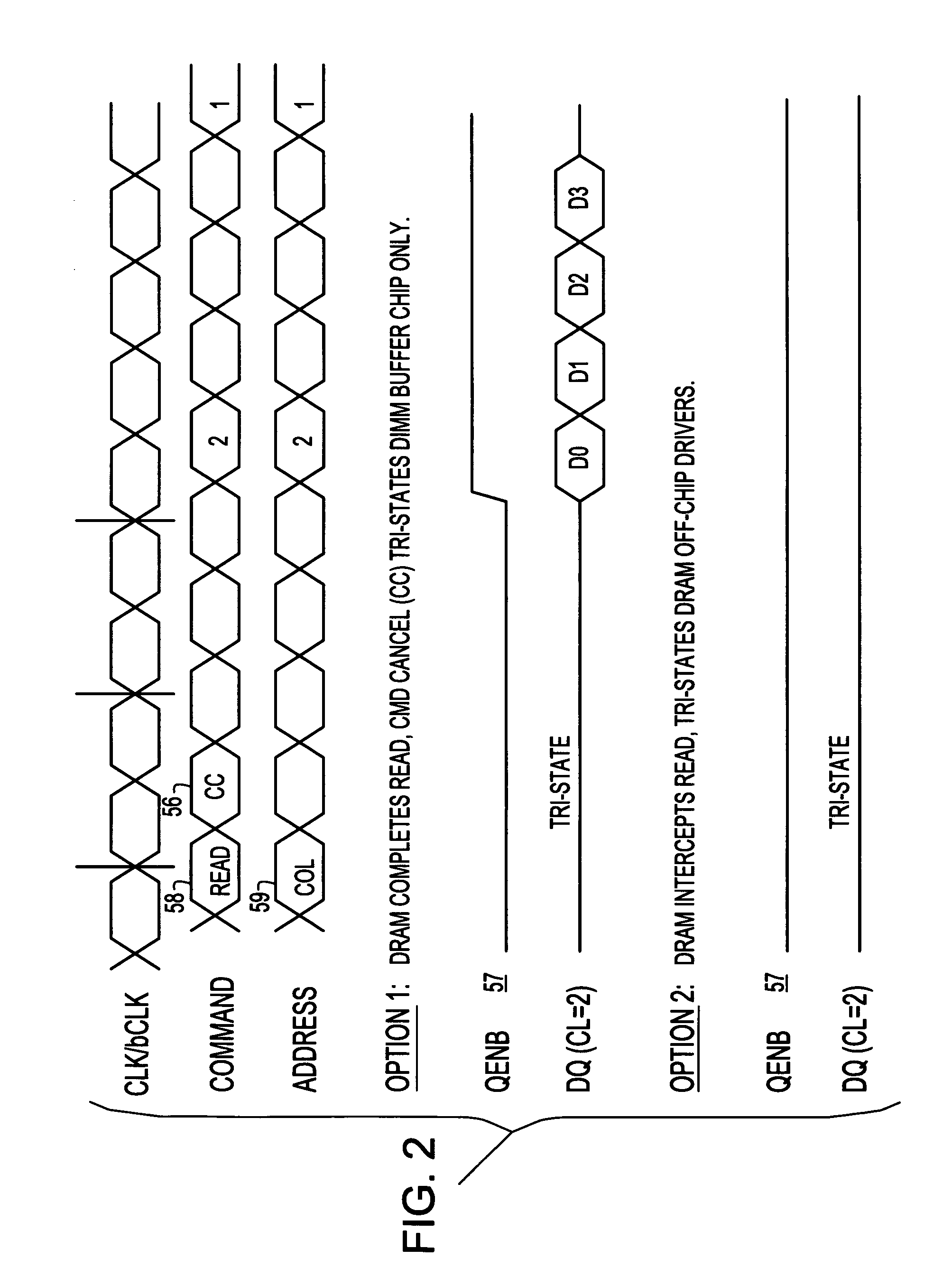
[0031]A DRAM implementation of the ‘command cancel’ operation mentioned above can be implemented via a command decode, or via one or more unique pins (to maximize coverage of command bus failures). It should be understood that this is not the only technique that is appropriate—since memory interfaces are periodically re-defined.

[0032]In summary, the operation of the present invention operates a novel Command Cancel (CC) system in both the read and write operations as follows:

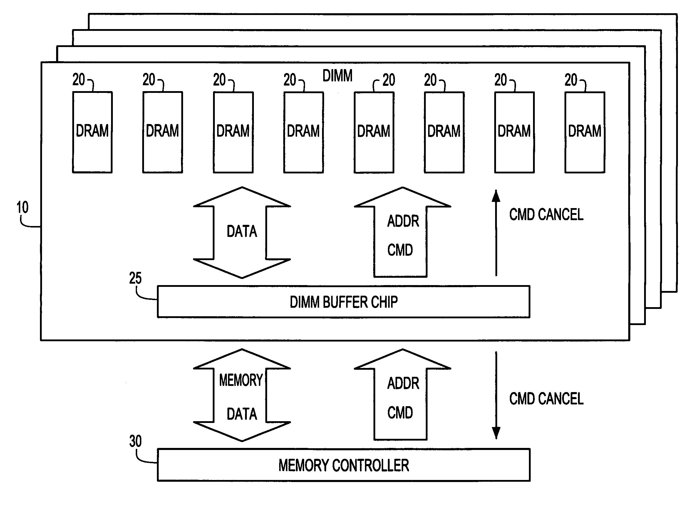
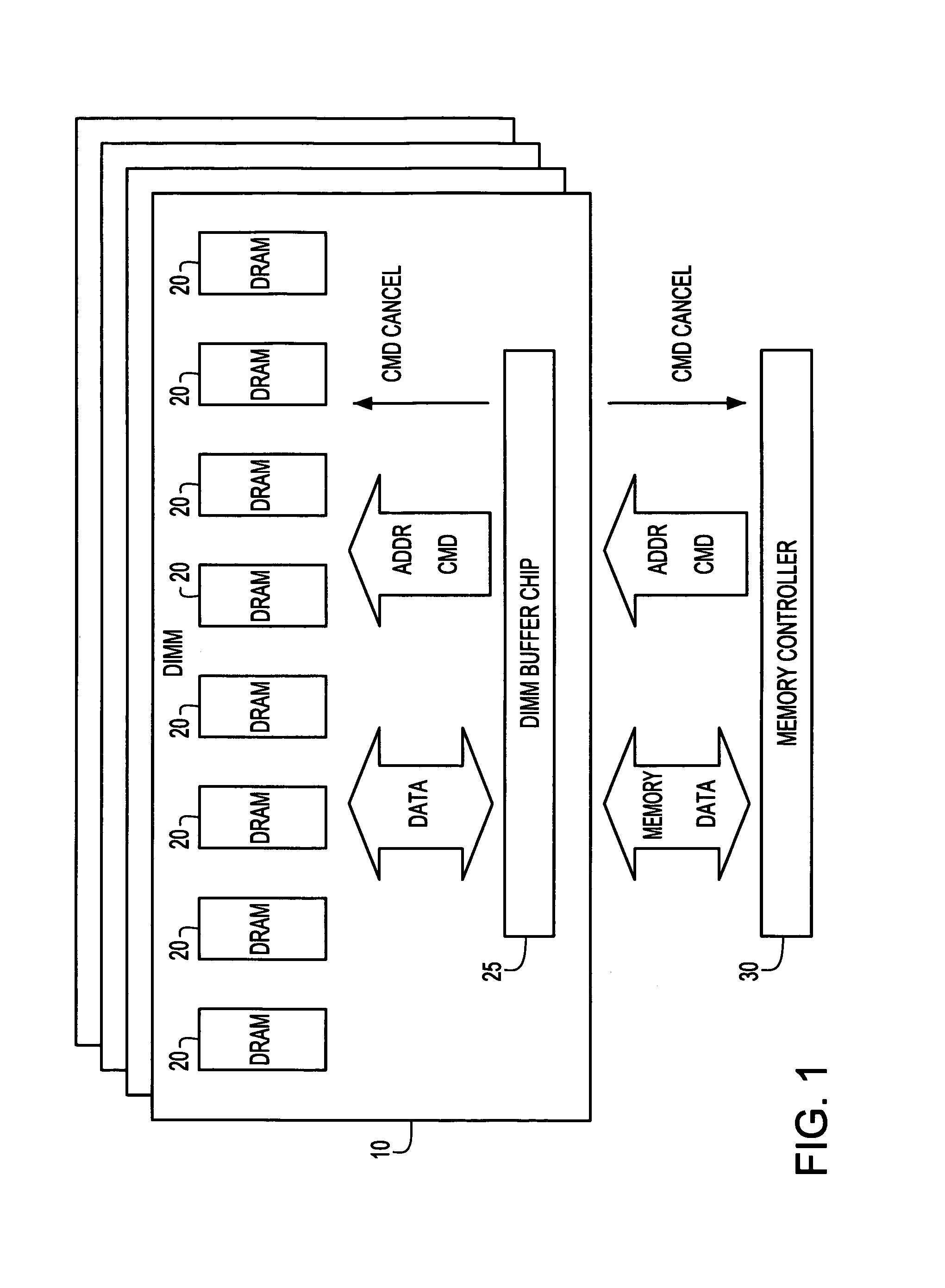
[0033]Attention is directed to FIG. 1 which illustrates number of memory modules 10 known as dual in-line memory modules (DIMMS) on which number of Dynamic Random Access Memory 20 (DRAM) and a buffer chip 25 are mounted in a known manner.

[0034]The buffer chip receives address commands from an external memory controller or chip 30 and transmits the commands to the DRAMs 20. The memory data is likewise transmitted and received from the memory controller 30 to the buffer chip 25 to and from the DRAMs 20. It should ...


PUM


Abstract

A method for performing a common cancel (CC) function on a dynamic random access memory (DRAM) semiconductor device to improve reliability and speed of a memory system. The CC function rakes advantage of the intrinsic delays associated wit memory read operations at high clock frequencies, and the increased write latency commensurate with increased read latencies where non-zero larencies for read and write operations are the norm by permitting address and command ECC structures to operate in parallel with the address and command re-drive circuitt The CC function is extendable to future DDR2 and DDR3 operating requirements in which latency of higher frequency modes will increase due to the shift from 2 bit pre-fetch to 4 and 8 bit pre-fetch architecture.

Description

BACKGROUND OF THE INVENTION[0001]The present invention relates generally to integrated circuit memory devices and, more particularly, to a synchronous dynamic random access memory (SDRAM) system.[0002]Problems in state of the art memory systems have been because of intrinsic delays associated with memory read operations at high clock frequencies, and the increased write latency commensurate with increased read latencies, where non-zero latencies for read and write operations are the norm. In the case of ‘read’ operations, this data latency will be directly associated with the amount of time required to access the data from the sense amplifier latch or other intermediate storage location—typically 3 or 4 clocks at a 266 MHz clock speed. In the case of ‘write’ operations, whereas it is still theoretically possible to provide data and address at the same time, data will typically be delayed several clocks after address, to improve command / address bus efficiency and reduce SDRAM power—s...

Claims


Application Information

Patent Timeline
IPC IPC(8): G06F12/00G06F11/10G06F12/02G06F12/16G11C7/10G11C7/22G11C11/40G11C11/401G11C11/4076G11C11/408G11C11/4093
CPCG06F11/1016G11C7/1072G11C7/1078G11C7/109G11C7/22G11C11/4076G11C11/408G11C11/4093G11C2207/104B42D15/02B42D15/008
Inventor ELLIS, WAYNE F.KELLOGG, MARK W.PHIPPS, DANIEL J.
Owner MARVELL ASIA PTE LTD
Why Eureka
Try Eureka