Check patentability & draft patents in minutes with Patsnap Eureka AI!

System and method for providing high endurance low cost CMOS compatible EEPROM devices

Active Publication Date: 2009-01-27
NAT SEMICON CORP
View PDF6 Cites 23 Cited by
  • Summary
  • Abstract
  • Description
  • Claims
  • Application Information

AI Technical Summary

Problems solved by technology

A fundamental design challenge in creating a memory cell of an electrically erasable programmable read only memory (EEPROM) device is to use a controllable and reproducible electrical effect that has sufficient non-linearity so that the memory cell (1) can be written to (or erased) at one voltage in less than one millisecond (1 ms) and can be read at another voltage, and (2) the data within the memory cell must remain unchanged for more than ten (10) years.
These prior art requirements create process complexity and high cost when embedded into a complementary metal oxide semiconductor (CMOS) process.
This results in poor data retention and slower speeds for an EEPROM that comprises one PMOS program transistor and one PMOS control capacitor.
Hot electrons that pass through gate oxide will create oxide damage.
Oxide damage degrades the endurance of a memory cell.
Therefore, one major drawback to adding an extra capacitor is that it degrades EEPROM memory cell endurance performance.
Another drawback to adding an extra capacitor is that it significantly increases the size of the basic memory cell.
This significantly lowers the EEPROM array density.
This increases the cost.
Another drawback of prior art CMOS EEPROM technology is the speed of the programming procedure.
Because the efficiency of generating and injecting the drain avalanche hot electrons is low, programming times are relatively long.
However, the relatively high value for the coupling ratio leads to excess oxide damage.
However, some CMOS NVM memory cells were found to not meet the required levels of performance.
As the number of program / erase cycles increased, the number of failures (i.e., the number of “weak programmed” memory cells) also increased.
Lower program current inevitably causes “weak programmed” memory cells.
Decreasing the channel current during the programming process inevitably leads to the creation of “weak programmed” memory cells.
Large variations in program current (IG) may lead to increased stress in memory cells and cause early failure in the affected memory cells.
Although CMOS non-volatile memory (NVM) memory cells are relatively low in cost, they are capable of only about one thousand (1,000) program / erase cycles.
Although FLOTOX EEPROM devices have a high level of endurance, they are more complicated and more expensive.
The cost of embedding such an EEPROM device into a CMOS platform is rather high because many manufacturing process steps have to be changed or added to the basic CMOS process.
That is, the manufacturing process for the FLOTOX EEPROM devices is basically not CMOS compatible.
On the other hand, the cost of embedding CMOS compatible EEPROM devices into a CMOS platform is very low.
In CMOS non-volatile memory (NVM) devices, the Drain Avalanche Hot Carrier (DAHC) programming operation creates more oxide damage than does the Fowler-Nordheim (FN) programming operation.
In addition, because the programming operation and the erase operation are conducted through two transistor gate oxides (instead of one transistor gate oxide), the damage to the gate oxide of the transistors is shared between two transistors.

Method used


Image

  • System and method for providing high endurance low cost CMOS compatible EEPROM devices
  • System and method for providing high endurance low cost CMOS compatible EEPROM devices
  • System and method for providing high endurance low cost CMOS compatible EEPROM devices

Examples


Embodiment Construction

[0052]FIGS. 5 through 15, discussed below, and the various embodiments used to describe the principles of the present invention in this patent document are by way of illustration only and should not be construed in any way to limit the scope of the invention. Those skilled in the art will understand that the principles of the present invention may be implemented with any type of suitably arranged electrically erasable programmable read only memory (EEPROM) device.

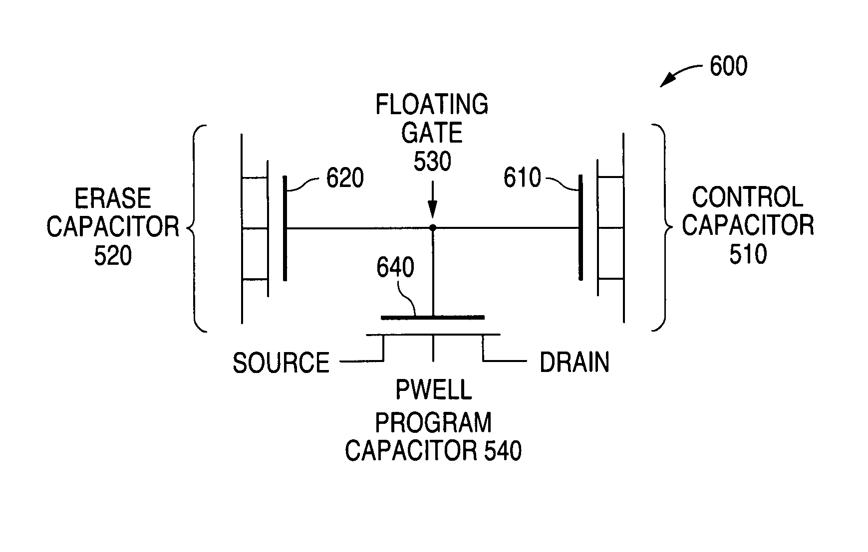
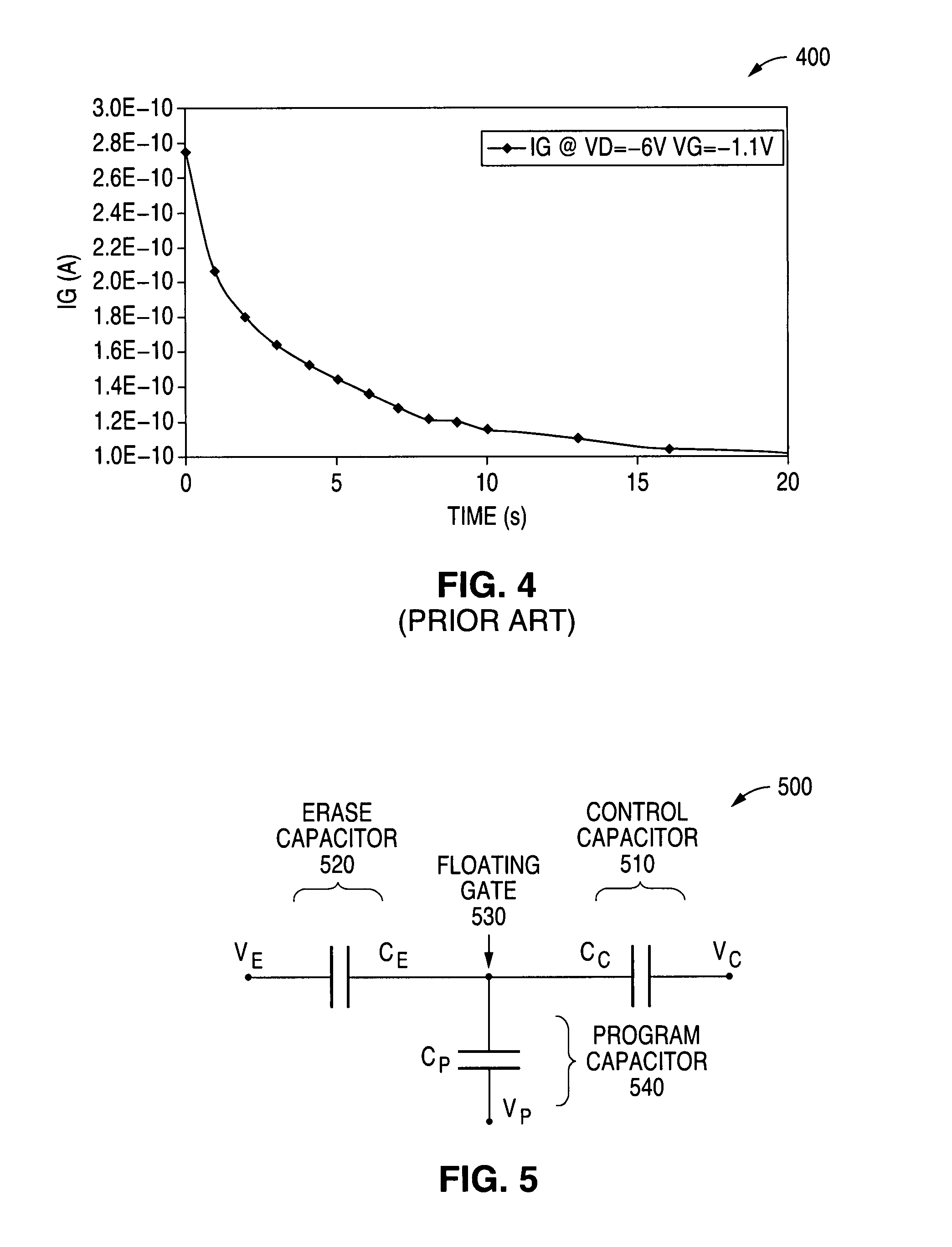
[0053]FIG. 5 illustrates a schematic diagram of one advantageous embodiment of a memory cell 500 of an electrically erasable programmable read only memory (EEPROM) device of the present invention. Memory cell 500 comprises control capacitor 510, erase capacitor 520, floating gate 530, and program capacitor 540 coupled together as shown in FIG. 5. As will be more fully discussed below, the program capacitor 540 also performs the function of a read transistor for the memory cell 500.

[0054]The control capacitor 510, the erase ...


PUM


Abstract

A system and method are disclosed for providing EEPROM devices that combine the high endurance features of complex and expensive EEPROM devices and the low manufacturing costs of CMOS compatible EEPROM devices. A memory cell of the invention comprises a control capacitor, an erase capacitor, and a program capacitor, each of which comprises an NMOS transistor. The gates of the three NMOS transistors are connected together to form a floating gate. The drain of the NMOS transistor of the program capacitor is separately connected so that the program capacitor can also serve as a read transistor. A memory cell of the invention can be programmed or erased in an array of memory cells without disturbing the other memory cells in the array.

Description

TECHNICAL FIELD OF THE INVENTION[0001]The present invention is generally directed to the manufacture of integrated circuits and, in particular, to a system and method for providing high endurance, low cost complementary metal oxide semiconductor (CMOS) compatible EEPROM devices.BACKGROUND OF THE INVENTION[0002]A fundamental design challenge in creating a memory cell of an electrically erasable programmable read only memory (EEPROM) device is to use a controllable and reproducible electrical effect that has sufficient non-linearity so that the memory cell (1) can be written to (or erased) at one voltage in less than one millisecond (1 ms) and can be read at another voltage, and (2) the data within the memory cell must remain unchanged for more than ten (10) years.[0003]Prior art stacked / split gate EEPROM technology requires (1) special multi-polysilicon materials, (2) different gate oxide thicknesses, and (3) modified doping profiles. These prior art requirements create process compl...

Claims


Application Information

Patent Timeline
IPC IPC(8): G11C16/04
CPCG11C16/0416H01L27/11519H01L27/11521H01L27/11558H01L29/7883G11C2216/10H10B41/10H10B41/60H10B41/30
Inventor BU, JIANKANG
Owner NAT SEMICON CORP
Features
  • R&D
  • Intellectual Property
  • Life Sciences
  • Materials
  • Tech Scout
  • Unparalleled Data Quality
  • Higher Quality Content
  • 60% Fewer Hallucinations
Learn More