
Wide dynamic range pinned photodiode active pixel sensor (APS)

a photodiode active pixel and dynamic range technology, applied in the field of pixel structure used in a cmos active pixel array, can solve the problems of high photodiode dark current, thermal noise, thermal noise, etc., and achieve good dynamic range and high illumination levels.

Active Publication Date: 2009-02-10
APTINA IMAGING CORP
View PDF30 Cites 42 Cited by
  • Summary
  • Abstract
  • Description
  • Claims
  • Application Information

AI Technical Summary

Benefits of technology

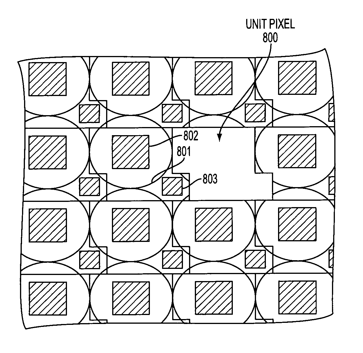
[0004]The present invention provides a pixel architecture which seeks to mitigate many of the noted drawbacks and employs a dual pixel pinned photodiode architecture operating in a dual charge integration. The two pixels enable a dual sensitivity pixel array in which one pixel functions to reproduce normal images, while the other pixel functions to reproduce images with high illumination levels. The dual charge integration mode and dual sensitivity, in combination, produce a pixel architecture having good dynamic range without having to resort to a logarithmic pixel architecture.

Problems solved by technology

However, conventional pixel architectures are subject to one or more of the drawbacks of high photodiode dark current, thermal (kTC) noise, fixed light sensitivity ratio and charge leakage.
Moreover, when logarithmic architectures are used to increase dynamic range, a more complicated color pixel processing is required.

Method used


Image

  • Wide dynamic range pinned photodiode active pixel sensor (APS)
  • Wide dynamic range pinned photodiode active pixel sensor (APS)
  • Wide dynamic range pinned photodiode active pixel sensor (APS)

Examples


first embodiment

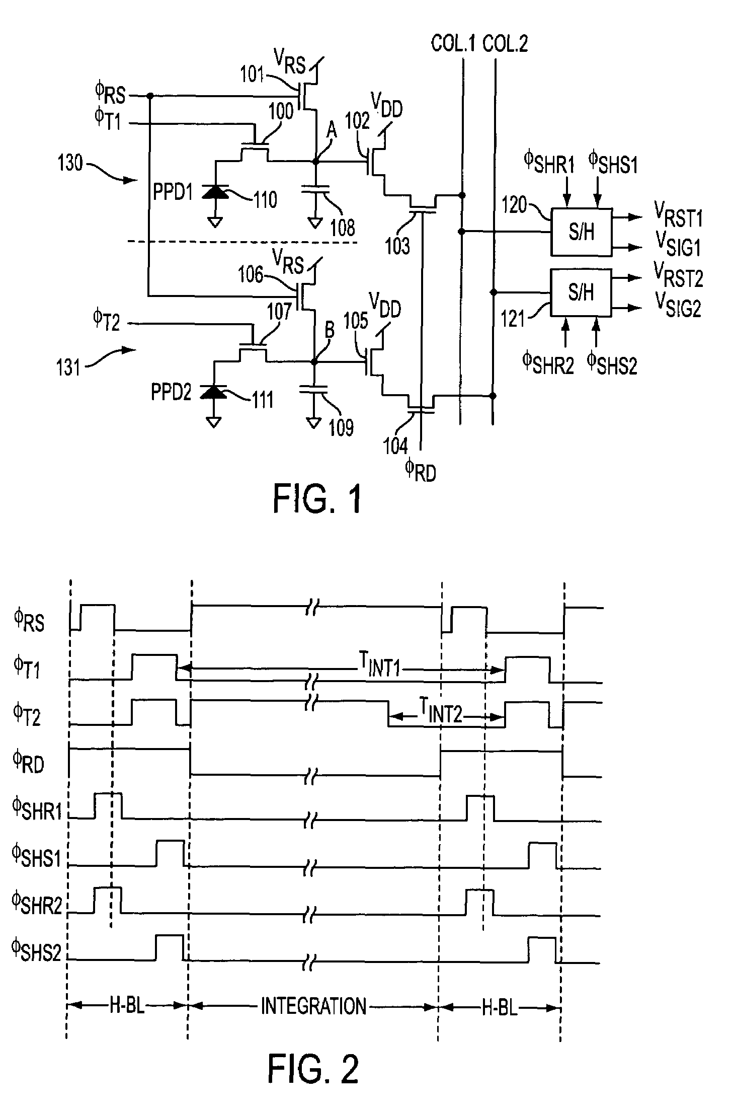
[0015]FIG. 1 illustrates the present invention, wherein the circuit comprises an upper pixel circuit 130 and a lower pixel circuit 131. The upper pixel circuit is defined by pinned photodiode PPD1 (110), transfer transistor 100, floating diffusion node “A,” a capacitor 108 coupled to node “A”, source follower transistor 102 having a gate connected to node “A” and a row select transistor 103. The pixel circuit includes a reset transistor 101, which operates in response to a reset pulse signal φRS applied to its gate. Row select transistor 103 is further coupled to the first of two column signal lines (COL. 1) and receives a row select pulse signal φRD at its gate. Transfer transistor 100 is responsive to a transfer pulse signal φT1 applied to its gate to transfer charge from the pinned photodiode 110 to diffusion node “A.” The upper pixel circuit is operated to handle “normal” light conditions (i.e., from low light to medium light levels) and has high sensitivity characteristics by u...

second embodiment

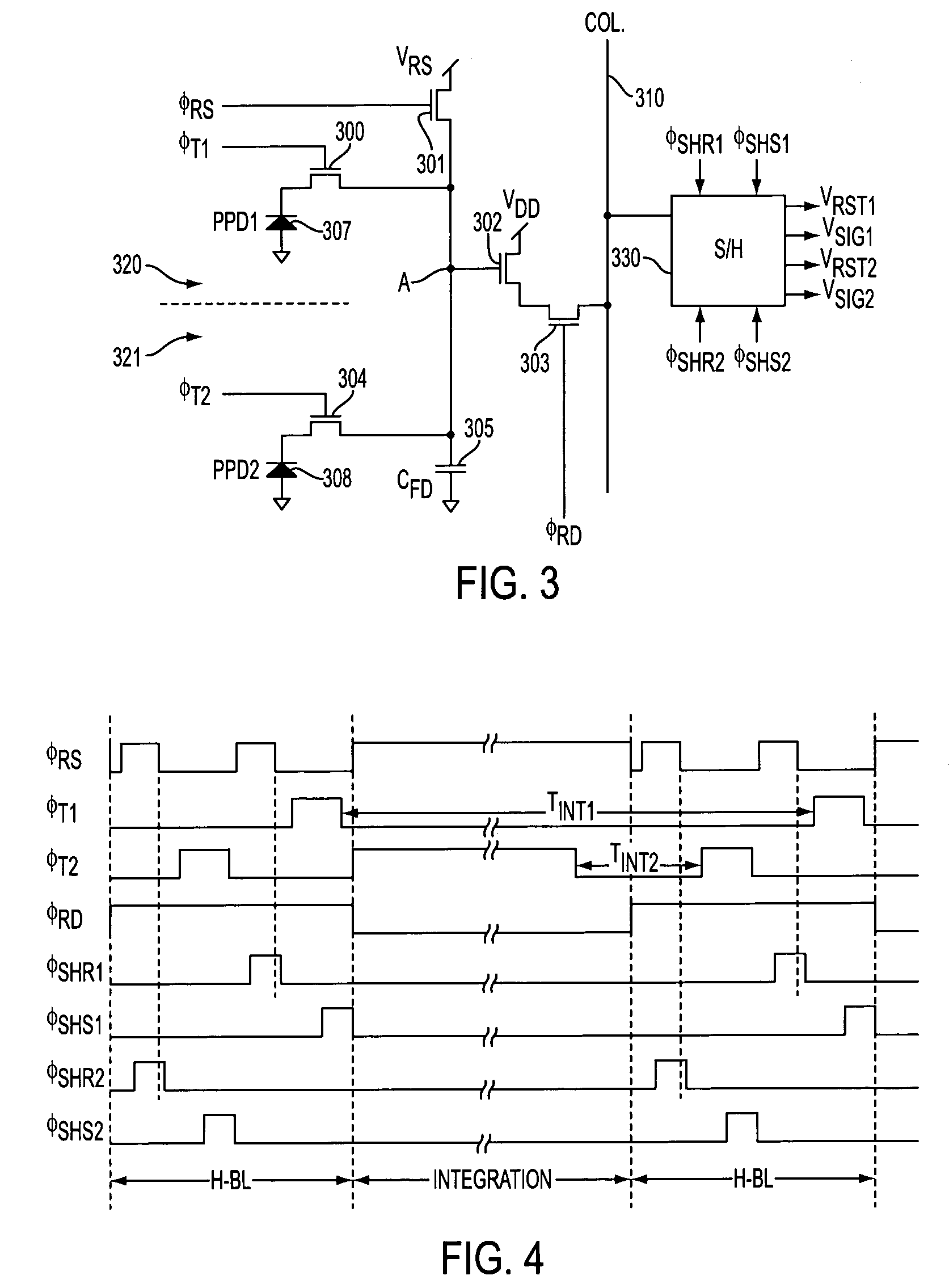
[0022]FIG. 3 illustrates the present invention, wherein one column signal line (310) is being used to output the signals from two pixels 320, 321. The circuit of FIG. 3 obtains two sets of output signals (VRST1, VSIG1; VRST2, VSIG2), and the charge transfer operation for the two pixels is performed sequentially (as shown by the timing diagram in FIG. 4).

[0023]The upper pixel circuit 320 of the pixel configuration includes a transfer transistor 300, having a source coupled to pinned photodiode PPD1307, a drain coupled to floating diffusion node “A,” a capacitor 305 having one terminal coupled to diffusion node “A” and to the drain of transfer transistor 300 and another terminal coupled to ground. An anode of pinned photodiode 307 is also coupled to ground. The gate of transfer transistor 300 receives transfer control signal φT1. Reset transistor 301 is coupled to both the upper and lower pixel circuits 320, 321 at node “A”, and is triggered by reset pulse signal φRS. The upper pixel ...

third embodiment

[0028]the present invention is illustrated in FIG. 5, where the circuit comprises an upper and lower pixel circuits 520, 521, with the upper pixel circuit 520 including pinned photodiode PPD1 (510), transfer transistor 502, coupled between the photodiode 510 and floating diffusion node FD1, and the capacitor 507 having one terminal connected to floating diffusion node FD1 and another terminal coupled to ground, reset transistor 500 coupled between a reset voltage VRS and node FD1, and capacitor 506 having one terminal coupled to capacitor 507 and the terminal coupled to a floating gate line 560 shared with lower pixel circuit 521. The reset transistor 500 receives a reset control signal φRS at its gate. The upper pixel circuit 520 provides an output on line 560 coupled to transistor 501 which has one side connected to voltage VRFG and another side connected to common floating gate line 560. The gate of transistor 501 receives a control signal φRFG.

[0029]The lower pixel circuit inclu...


PUM


Abstract

An image apparatus and method is disclosed for extending the dynamic range of an image sensor. A first linear pixel circuit produces a first pixel output signal based on charge integration by a first photo-conversion device over a first integration period. A second linear pixel circuit produces a second pixel output signal based on charge integration by a second photo-conversion device over a second integration period, where the second integration period is shorter than the first integration period. A sample-and-hold circuit captures signals representing the first and second pixel output signals.

Description

FIELD OF THE INVENTION[0001]The present invention relates to the pixel structure used in a CMOS active pixel array.BACKGROUND OF THE INVENTION[0002]The dynamic range (DR) for an image sensor is commonly defined as the ratio of the largest nonsaturating signal to the standard deviation of noise under dark conditions. The quality of an image sensor is largely defined by its dynamic range—as it increases, the sensor can detect a wider range of illuminations and consequently produce images of greater detail and quality.[0003]Several pixel architectures have been developed in an effort to produce good dynamic range. However, conventional pixel architectures are subject to one or more of the drawbacks of high photodiode dark current, thermal (kTC) noise, fixed light sensitivity ratio and charge leakage. Moreover, when logarithmic architectures are used to increase dynamic range, a more complicated color pixel processing is required.BRIEF SUMMARY OF THE INVENTION[0004]The present invention...

Claims


Application Information

Patent Timeline
Patent Type & Authority Patents(United States)
IPC IPC(8): H04N5/335G02B3/00H04N5/353H04N5/355H04N5/374H04N5/378
CPCH04N5/35554H04N5/35563H04N5/37457H04N25/583H04N25/585H04N25/778H04N25/78
Inventor NAKAMURA, JUNICHI
Owner APTINA IMAGING CORP
Learn More