High-temperature alloy standoffs for injection molding of solder

a technology of alloy standoff and solder, which is applied in the direction of soldering apparatus, sustainable manufacturing/processing, and final product manufacturing, etc., can solve the problems of large volume of chemical baths, impracticality of solder paste screening techniques, and high cost, and achieves convenient manufacturing, accurate control, and economical

Inactive Publication Date: 2009-03-24
IBM CORP
View PDF7 Cites 10 Cited by
  • Summary
  • Abstract
  • Description
  • Claims
  • Application Information

AI Technical Summary

Benefits of technology

[0009]Pursuant to the invention, standoffs are automatically formed in those particular cavities containing the high-temperature solder to the required precise size, and which can be accurately controlled. These standoffs are produced utilizing currently available standard manufacturing techniques, and are readily manufacturable employing bulk processing in an inexpensive, economical manner.

Problems solved by technology

Another method employs electroplating of solder, which requires large volumes of chemical baths and which is especially hazardous due to the fact that many solders contain lead.
However, with the recent trend in the miniaturization of device dimensions and the reduction in bump-to-bump spacing (or pitch), the solder paste screening technique becomes impractical.
For instance, one of the problems in applying solder paste screening technique to modem IC devices is the paste composition itself, in that this is generally composed of a flux and solder alloy particles.
The consistency and uniformity of the solder paste composition becomes more difficult to control with a decreasing solder bump volume.
However, some problems have been encountered when the technique is implemented to wafer-sized substrates.
However, as the load increases, the standoff will be decreased to the point of contact between the nearest points, such that can reduce the integrity of the connection between the components.

Method used


Image

  • High-temperature alloy standoffs for injection molding of solder
  • High-temperature alloy standoffs for injection molding of solder

Examples


Embodiment Construction

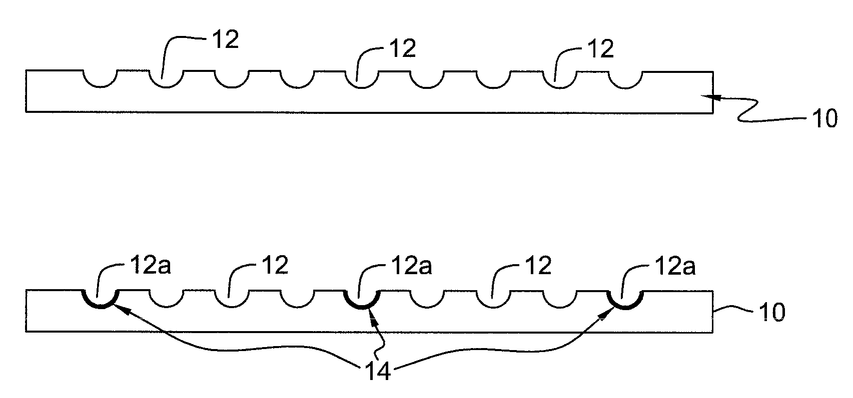
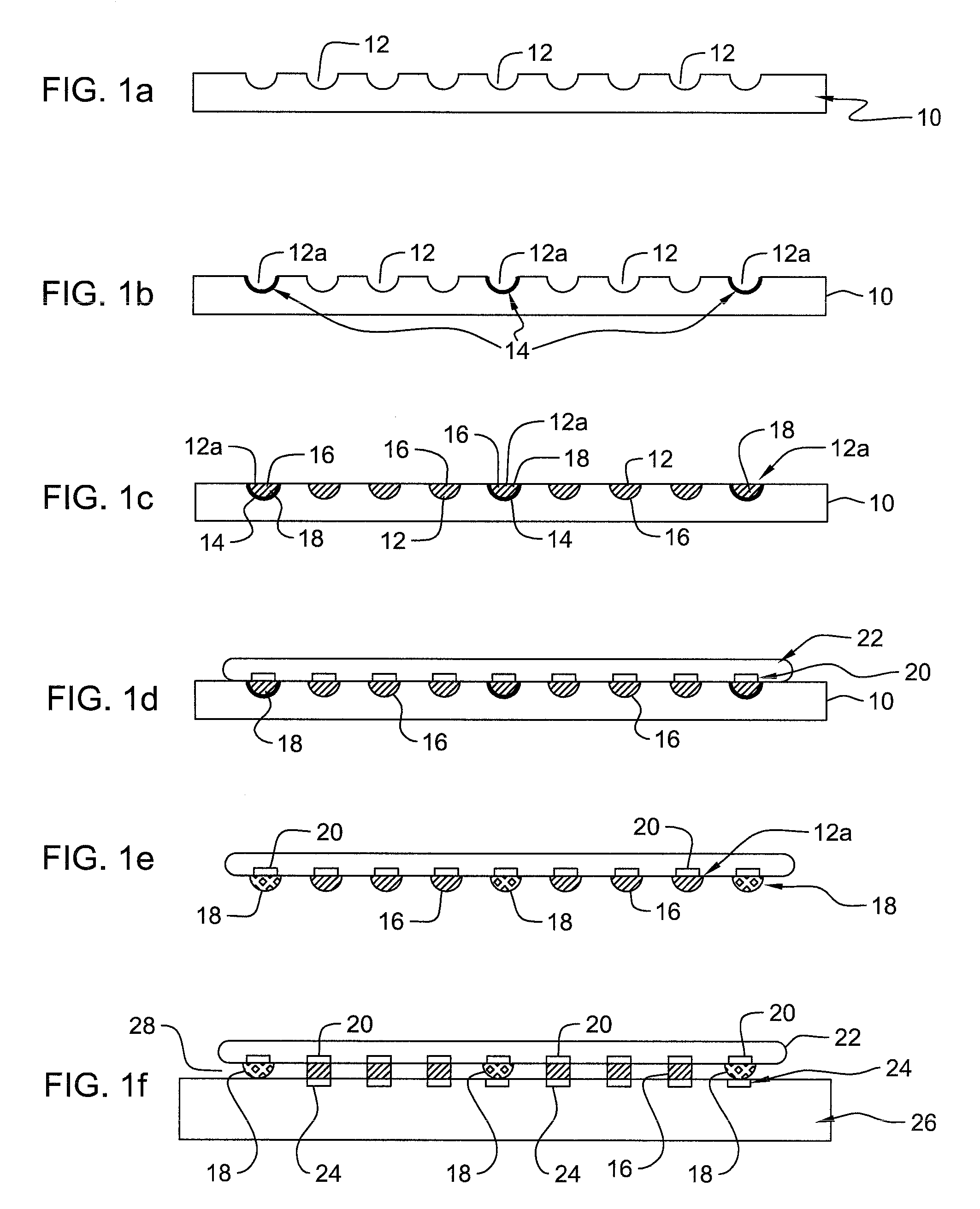
[0013]Referring now in detail to the illustrated embodiment of the inventive method, as represented in FIGS. 1a through 1f of the drawings, FIG. 1a illustrates an essentially standard injection molded solder mold 10 incorporating a plurality of cavities 12, which in this case are hemispherical in shape, although other shapes are contemplatable. The mold, as is well known in the technology, is generally formed of a suitable dielectric material, such as a boro-silicate glass, or the like.

[0014]As indicated in FIG. 1b of the drawings, at various locations, some of the cavities 12a are lined with a metal 14, preferably, but not necessarily, employing a shadow mask or sputtering technique.

[0015]All of the cavities 12, 12a in the mold 10, as illustrated in FIG. 1c of the drawings, are then filled with a solder 16, employing standard techniques, and wherein the solder 16 will then alloy with the metal 14 in the selected cavities 12a of FIG. 1b, so as to produce a higher temperature solder ...


PUM

PropertyMeasurementUnit
temperatureaaaaaaaaaa
densitiesaaaaaaaaaa
volumesaaaaaaaaaa

Abstract

A method in forming high-temperature alloy solder standoff in a solder bumping process, such as in injection molded solder molds. The standoffs are formed in an injection molded solder mold, by means of pre-depositing a layer of a metal at select sites, such as some of the cavities which are formed in the surface of the mold, and thereafter, filling the mold cavities with solder, utilizing standard techniques as known in the technology. The particular metal, which is deposited in at least some of the mold cavities, will alloy with the solder during or after transfer, and will result in the formation of a higher temperature alloy solder at select locations in the mold cavities.

Description

BACKGROUND OF THE INVENTION[0001]1. Field of the Invention[0002]The present invention generally pertains to the injection molding of solder, and more particularly relates to a method in the formation of high-temperature alloy solder standoff in a solder bumping process, such as in injection molded solder molds.[0003]2. Discussion of the Prior Art[0004]In modem semiconductor devices, the ever-increasing electronic component densities on the devices and reduced dimensions of the devices demand more stringent requirements in the packaging or interconnecting techniques thereof. Generally, a known flip-chip attachment method has been used in the packaging of IC chips, wherein a formation of solder balls was carried out by an evaporation method of lead and tin through a mask for producing the desired solder balls. Another method employs electroplating of solder, which requires large volumes of chemical baths and which is especially hazardous due to the fact that many solders contain lead....

Claims


Application Information

Patent Timeline
Patent Type & Authority Patents(United States)
IPC IPC(8): H05K3/34H01L21/00H01L23/488
CPCB23K3/0623H01L21/6835H01L24/11H01L24/12H01L24/742H01L24/81H05K3/3436H05K3/3478H01L2224/0401H01L2224/06505H01L2224/11003H01L2224/13099H01L2224/14505H01L2224/81136H01L2224/81801H01L2924/01082H01L2924/14H05K3/3463H05K2201/09781H05K2201/2036H05K2203/0113H05K2203/0338H01L2924/01033H01L2924/0105H01L2924/014H01L2924/10253H01L2924/00H01L2224/11334Y02P70/50
Inventor CORDES, STEVEN A.GRUBER, PETER A.
Owner IBM CORP
Why Eureka
Try Eureka