
Passive mode-locked semiconductor laser diode, and optical clock signal extracting device

a semiconductor laser diode and modelocked technology, applied in the direction of electromagnetic transmission, electromagnetic lasers, apparatus using atomic clocks, etc., can solve the problems of deteriorating optical signal quality, difficult for electronic devices to extract clock signals, and distortion generation of frequency and time-pulse waveforms to become more remarkable problems

Inactive Publication Date: 2009-03-24
OKI ELECTRIC IND CO LTD
View PDF10 Cites 6 Cited by
  • Summary
  • Abstract
  • Description
  • Claims
  • Application Information

AI Technical Summary

Benefits of technology

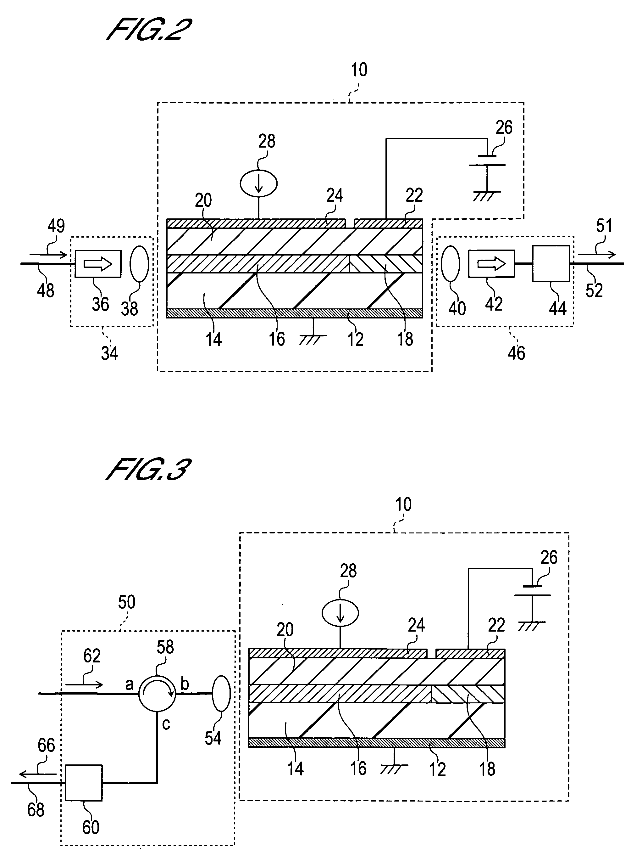
The present invention relates to a passive mode-locked semiconductor laser diode with a gain region and a saturable absorption region, which can generate an optical clock signal with high accuracy. The invention satisfies the conditions that the optical gain for polarization in the gain region is larger than the optical gain for TM polarization, and that the absorption saturation energy for TM polarization is smaller than the absorption saturation energy for TE polarization. The invention also includes an optical circulator and a coupling optical system to filter out unwanted light and improve the accuracy of the optical clock signal. The invention can be used in a variety of optical clock signal extracting devices.

Problems solved by technology

Along with development of the longer-distance transmission, optical losses on an optical transmission line, reduction in signal-to-noise ratio, wherein the reduction is caused by use of multistage optical amplifier, the group velocity dispersion of an optical fiber, and generation of a waveform strain depending on nonlinear optical-effects in the optical fiber have raised a problem that the quality of an optical signal is deteriorated.
The larger transmission capacity has caused distortion generation of frequency and time-pulse waveforms to become a more remarkable problem.
When the bit rate of the multiple signal exceeds 40 Gbit / s, it becomes difficult for an electronic device to extract an clock signal.
However, there is caused a problem, in the above-described first through fifth methods, that extracting operation of an optical clock signal strongly depends on the plane of polarization of the input optical signal.
That is, the extracting operation of the optical clock signal becomes unstable by the time fluctuation of the plane of polarization of the input optical signal.
However, when the both directions of the planes of polarization are orthogonal to each other, there is caused a situation in which no optical clock signal is extracted.
That is, when the optical clock signal is extracted from the input optical signal, there is a problem that there is generated the dependence on the plane of polarization of the input optical signal, that is, the optical clock signal is extracted in a stable manner when the input optical signal is TE polarization, and the optical clock signal may not be extracted in the case of the TM polarization.
That is, it is meant that the optical clock signal may not be extracted in a stable manner.

Method used


Image

  • Passive mode-locked semiconductor laser diode, and optical clock signal extracting device
  • Passive mode-locked semiconductor laser diode, and optical clock signal extracting device
  • Passive mode-locked semiconductor laser diode, and optical clock signal extracting device

Examples


Embodiment Construction

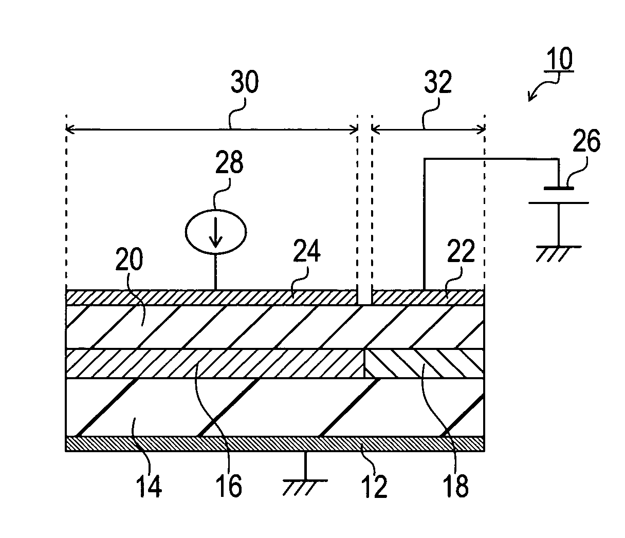
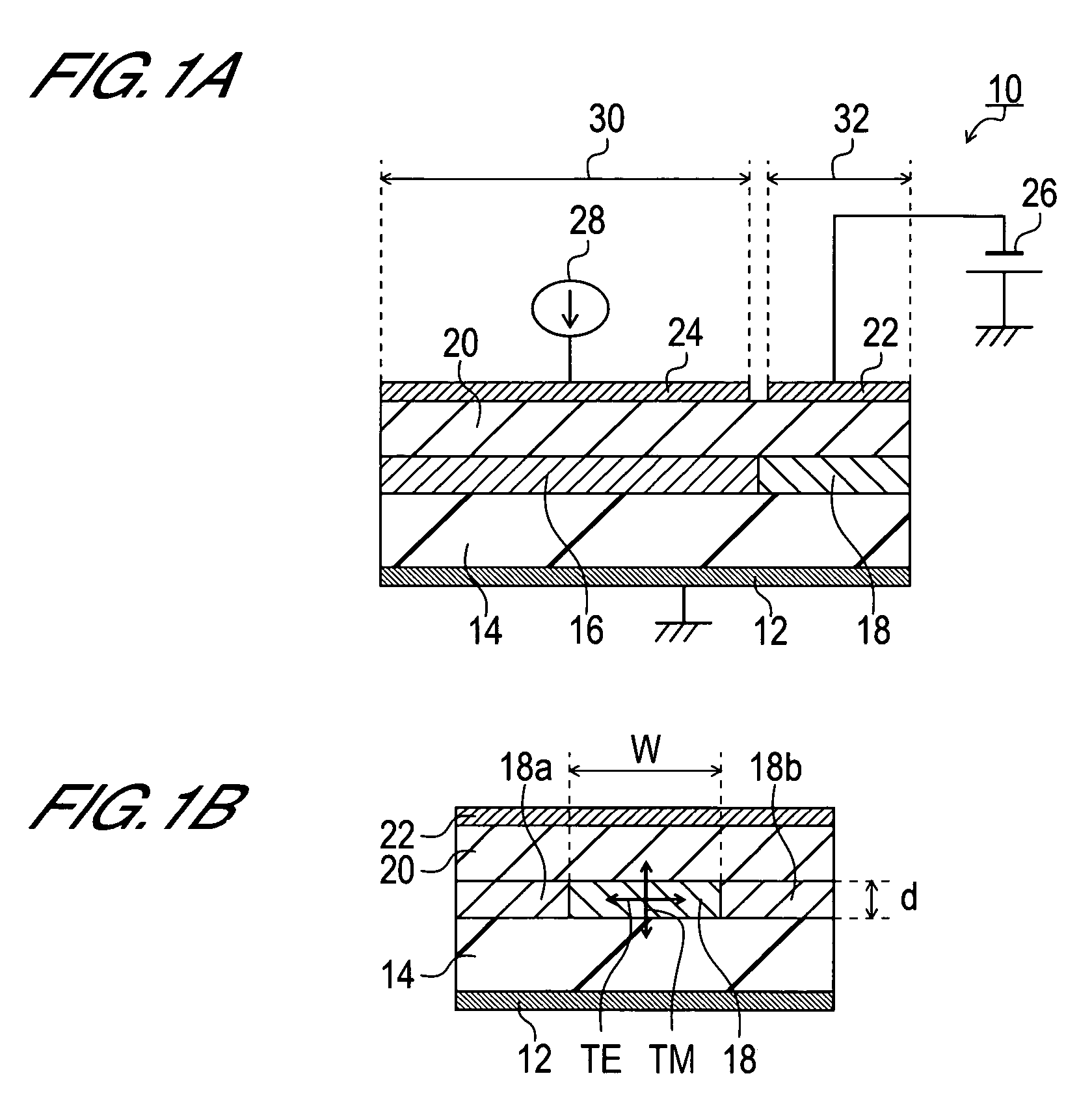
[0096]Hereinafter, embodiments according to the present invention will be explained, referring to drawings. Here, each of the drawings illustrates a configuration example according to the present invention, and is only a schematic view showing the arrangement of members and the like for easy understanding of the present invention, and the present invention is not limited to the illustrated examples. Moreover, though specific materials and conditions, and the like will be used in the following explanations in some cases, the above materials and conditions are only preferable examples, and, accordingly, the present invention will not be limited to the materials and conditions. Moreover, duplicated explanations of similar members throughout the drawings will be eliminated in some cases. Moreover, an optical path will be shown by a thick line, and a transmission line for an electric signal will be shown by a thin line.

[0097]

[0098]The structure of the passive mode-locked semiconductor la...


PUM


Abstract

To provide an optical clock signal extracting device with a simple configuration, by which an optical clock signal may be extracted without depending on the polarization direction of an input optical signal. A current is injected to a gain region 30 through an n-type common electrode 12 and a p-type electrode 24 in the gain region 30 by a constant current source 28. A reverse-bias voltage is applied by a constant voltage source 26 to a saturable absorption region 32 through the p-type electrode 12 and the n-type common electrode 72 in the saturable absorption region 32. An optical waveguide 16 in the gain region is formed with bulk crystal or a quantum well structure into which extension strain is introduced, and an optical waveguide 18 in the saturable absorption region is formed with a quantum well structure into which extension strain is introduced. Moreover, in the gain region, an optical gain for the TE mode is configured to be larger than that for the TM mode, and, in the saturable absorption region, absorption saturation energy for the TM mode is configured to be smaller than absorption saturation energy for the TE mode.

Description

BACKGROUND OF THE INVENTION[0001]1. Field of the Invention[0002]The present invention relates to a passive mode-locked semiconductor laser diode, and an optical clock signal extracting device using the diode.[0003]2. Description of Related Art[0004]In an optical communication network, longer-distance and larger-capacity transmission has been developed. Along with development of the longer-distance transmission, optical losses on an optical transmission line, reduction in signal-to-noise ratio, wherein the reduction is caused by use of multistage optical amplifier, the group velocity dispersion of an optical fiber, and generation of a waveform strain depending on nonlinear optical-effects in the optical fiber have raised a problem that the quality of an optical signal is deteriorated. The larger transmission capacity has caused distortion generation of frequency and time-pulse waveforms to become a more remarkable problem.[0005]Therefore, there have been provided repeaters at interva...

Claims


Application Information

Patent Timeline
Patent Type & Authority Patents(United States)
IPC IPC(8): H01S3/10H01S3/098B82Y20/00H01S5/065
CPCB82Y20/00H04L7/0075G04F5/14H01S5/0601H01S5/0609H01S5/0657H01S5/125H01S5/3201H01S5/34
Inventor ARAHIRA, SHIN
Owner OKI ELECTRIC IND CO LTD
Learn More