Method for surface cleaning

a surface cleaning and surface technology, applied in the direction of metallic material coating process, chemical vapor deposition coating, fluid pressure measurement, etc., can solve the problems of affecting the performance of the end product, occupying significant and costly floor space, complex equipment to deliver these chemicals in the ic industry, etc., to facilitate the state change of unwanted contaminants and facilitate removal.

Inactive Publication Date: 2009-04-07
UVTECH SYST
View PDF159 Cites 26 Cited by
  • Summary
  • Abstract
  • Description
  • Claims
  • Application Information

AI Technical Summary

Benefits of technology

[0008]The preferred embodiments of the present invention relate generally to a system and methods for surface cleaning and more particularly to removal of unwanted films, or contaminants, such as photoresist, post-etch residues and particles using optical energy in the visible or near-visible spectrum in conjunction with a gas to facilitate a state change in these unwanted contaminants such that removal is facilitated, without damage to the surface on which these unwanted contaminants reside.
[0010]In a preferred embodiment, the system in accordance with the present invention includes a solid state laser having wavelengths with low photon energies in a near-visible (also called “black light” or “near-UV”) portion of the electromagnetic spectrum, as well as visible light, defined as light visible to the human eye. Near-visible is herein defined as wavelengths in the range of 300-400 nm and visible as 380-780 nm. Use of such a laser greatly minimizes damage to the substrate during cleaning. In addition, a gas having low UV absorption properties is employed to facilitate direct oxidization with little or no photoionization. Use of such a gas helps reduce the risk of damaging sensitive substrates such as substrates having a low dielectric constant. Light sources having low powered pulses with pulse energies of less than 1 mJ are employed to facilitate photochemically driven reactions. These types of pulses are also more selective at targeting photoresist and contaminants and have fewer thermal effects as compared to higher powered pulse energies associated with other cleaning techniques.
[0011]Embodiments of the invention also employ high laser pulse repetition rates in the range of 1 kHz to 100 kHz to facilitate continual production of reactive species and more complete combustion of the contaminant as well as preventing carbon re-deposition during cleaning.
[0012]Preferred embodiments of the present invention include a high concentration of ozone to facilitate more reactive oxidation, higher rate of resist removal and complete carbon removal without requiring the use of water. For example, embodiments of the present invention can employ ozone concentrations in the order of approximately 15% by weight, and carbon removal to the limit of detectability.
[0013]In preferred embodiments, water vapor injection is used to enhance production of radical oxygen atoms and hydroxyl (OH) radicals. Water vapor injection also makes the gas reaction zone (GRZ) more effective. Embodiments of the invention can employ water vapor injection rates on the order of 250 sccm. Furthermore, substrates can be cleaned at low temperatures on the order of 90° C. to 110° C. which reduces thermal stresses on the substrate and prevents warpage of the wafer.
[0015]In accordance with still another aspect of the invention, an apparatus for removing residue from the surface of a substrate is provided. The apparatus includes a holder for retaining the substrate using a negative pressure and for heating the substrate to facilitate removal of the residue. The apparatus also includes a substrate delivery module for placing the substrate on the holder and for removing the substrate after residue has been removed. A chamber surrounding the holder is capable of providing a hermetically sealed environment surrounding the surface of the substrate. In addition, the chamber has a window for allowing radiation to pass through while sufficiently illuminating the substrate surface. The apparatus also includes a gas delivery module for delivering a gas flow to the chamber as well as a laser for illuminating the surface of the substrate. The illumination, input gas and residue facilitate a reaction. The reaction is such that it causes the residue to change state from an essentially solid form to primarily a gaseous form. This state change causes the residue to be removed from the surface of the substrate.

Problems solved by technology

Failure to remove these residues may produce results which range from degraded performance of the end product to complete failure.
Surface cleaning during various manufacturing processes is a major component of cost that needs to be minimized.
The equipment to deliver these chemicals in the IC industry is complex, expensive, and occupies significant and costly floor space.
These contribute to high initial capital costs.
Additional facility costs are added, including floor space, plumbing for gases and air control, waste treatment and disposal.
Lastly, cost of ownership (CoO) expenses, including spare parts, maintenance, and labor, is added.
The equipment required to deliver, recapture, and process these chemicals is expensive and occupies costly floor space in the manufacturing area.
In addition to high equipment and chemical costs, these cleaning techniques often produce unwanted by-products that are considered hazardous and thus may have high disposal costs associated therewith.
The most significant cost in wafer cleaning is that related to ultrapure water.
Wet removal techniques may further damage the delicate and intricate surfaces of the manufactured products because of the corrosive and / or abrasive nature of the cleaning media.
Many of the dry removal techniques used in the art may fail to sufficiently clean a surface, may take a long time to remove adequate quantities of undesired products such as ion implanted resist or contaminants, may be difficult to operate, may be costly to operate, may damage the surface of the manufactured item, may require wet cleaning to remove carbon-based residues generated by the dry removal technique, may generate hazardous materials or substances and may require gases that are harmful to the environment if not handled and / or processed safely.

Method used


Image

  • Method for surface cleaning
  • Method for surface cleaning
  • Method for surface cleaning

Examples


Embodiment Construction

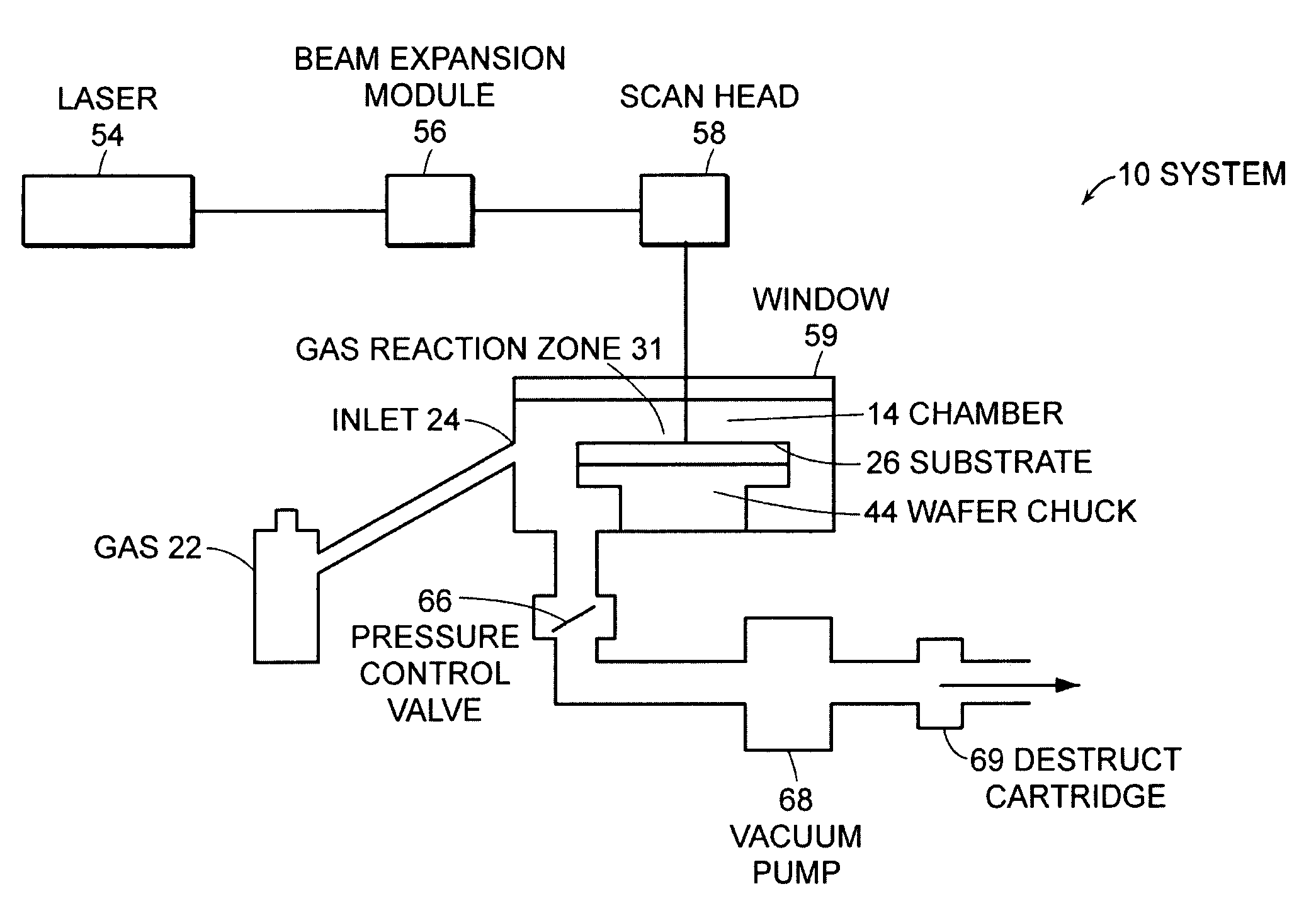
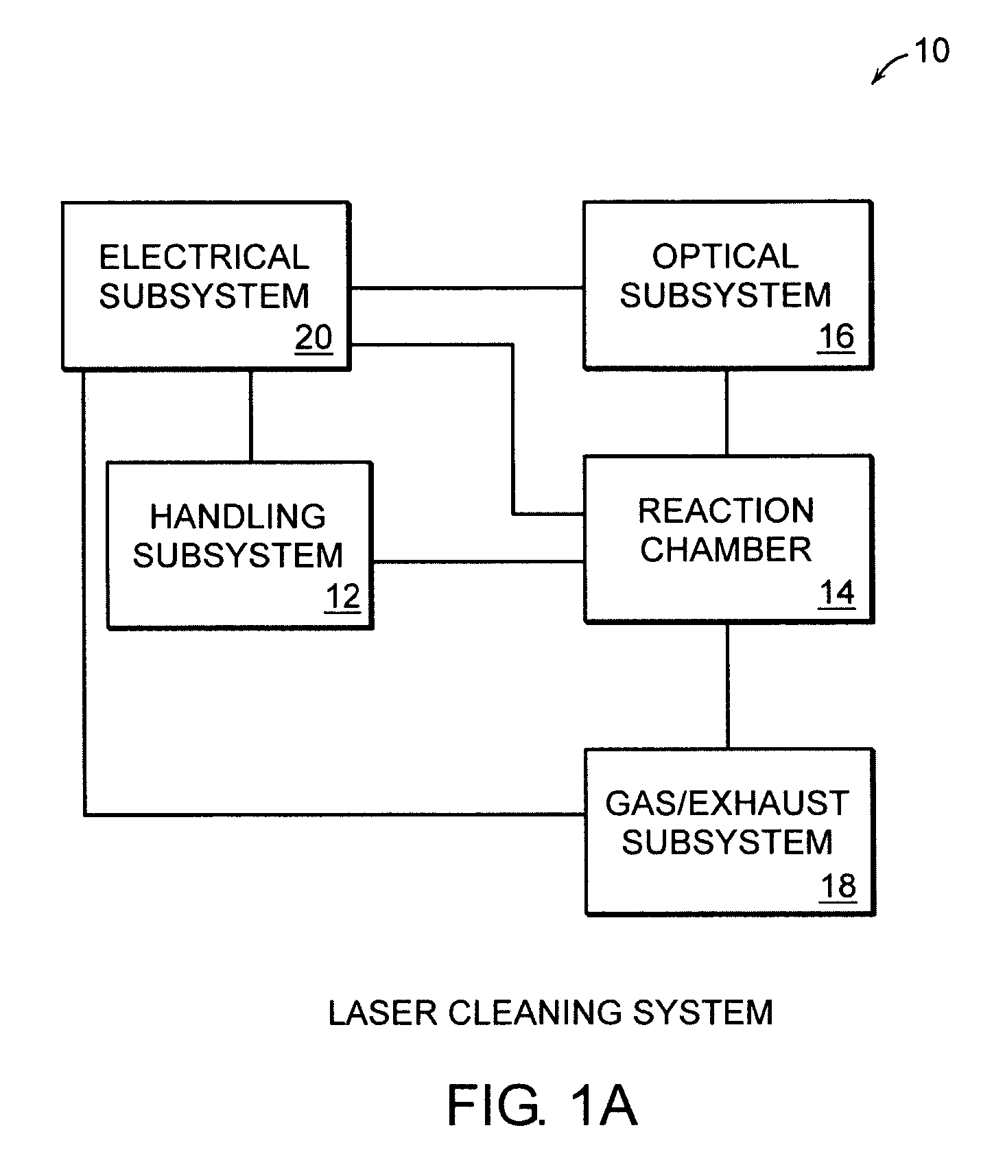
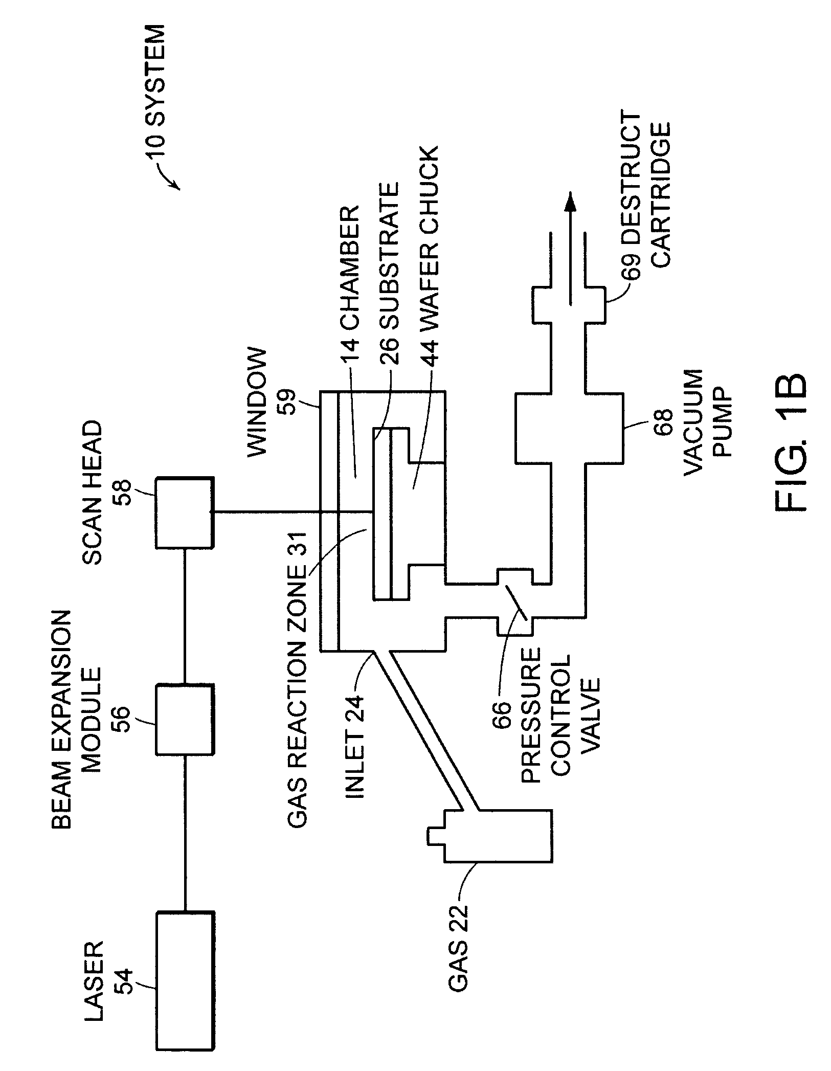
[0035]A preferred embodiment of the present invention consists of an automated, low cost, all-dry cleaning system that employs small volumes of oxygen, ozone and water vapor to remove photoresist and other organic residues, or matter, in a single step using a small laser emitting primarily 355 nm near-visible and residual 532 nm visible radiation wavelengths. By using embodiments of the invention, the surfaces of substrates are cleaned without leaving detectible roughening or detectible carbon residues. Substrate as used herein refers to any essentially planar surface having unwanted materials or substances disposed thereon. An example of a substrate is, but not limited to, a silicon wafer. For example, in one post cleaning test and analysis, the average carbon remaining from multiple readings was 3.27 Å. Use of a preferred embodiment of the invention also facilitates environmentally sound operations because no hazardous by-products requiring special handling or treatment are genera...


PUM

PropertyMeasurementUnit
wavelengthsaaaaaaaaaa
pulse energiesaaaaaaaaaa

Abstract

A system for removing photoresist from semiconductor wafers is disclosed. The system utilizes a solid-state laser having wavelengths in the near-visible and visible portions of the electromagnetic spectrum to remove photoresist without requiring hazardous gases or wet solutions. In addition, the system does not damage the substrate being cleaned, nor leave a carbon residue requiring further processing to remove. The system uses photon energy, oxygen, water vapor and ozone to interact with contaminants on a surface, forming a gas reaction zone (GRZ). The GRZ reacts and completely removes the photoresist or other unwanted contamination.

Description

CROSS REFERENCES TO RELATED APPLICATIONS[0001]The present application is a divisional application of U.S. patent application Ser. No. 10 / 870,646, filed Jun. 17, 2004 now abandoned.[0002]The entire content of the above application is incorporated herein by reference in entirety.BACKGROUND OF THE INVENTION[0003]The manufacture of electronic components and devices involves many processes, or steps, to produce an acceptable final product. Examples of electronic devices and components include, but are not limited to, integrated circuits (ICs), compact disks (CDs), thin film heads (TFHs), and related optoelectronic devices. The processes involved in making these devices and components are for example, but not limited to, annealing, oxidation, recrystallization, ultraviolet (UV) curing, surface conditioning, photo-assisted decomposition and etching, bacteria removal, and electrochemical decomposition. Many of these, especially photolithography, leave behind residues or resist films that mu...

Claims


Application Information

Patent Timeline
Patent Type & Authority Patents(United States)
IPC IPC(8): H01L21/00C23C14/00C23C16/00B08B3/12B08B7/00C23F1/00G03F7/42H01L21/311
CPCB08B7/0042G03F7/427H01L21/31138H01L21/67005
Inventor ELLIOTT, DAVID J.MILLMAN, JR., RONALD P.TARDIF, MURRAYAIELLO, KRISTA
Owner UVTECH SYST
Why Eureka
Try Eureka