Method for manufacturing a droplet ejection head

a technology of droplet ejection and droplet ejection, which is applied in the direction of recording equipment, instruments, and recording information storage, etc., can solve the problems of reduced yield, increased manufacturing cost, and cracking or chipping of silicon substrate during manufacturing steps, and achieves high printing performance.

Active Publication Date: 2009-05-26
SEIKO EPSON CORP
View PDF6 Cites 5 Cited by
  • Summary
  • Abstract
  • Description
  • Claims
  • Application Information

AI Technical Summary

Benefits of technology

[0015]It is an object of the present invention to provide a method for manufacturing a droplet ejection head with high yield, the droplet ejection head being prevented from being cracked or chipped during manufacturing steps; a droplet ejection head, manufactured by the method, having high ejection performance; and a droplet ejection apparatus, including the droplet ejection head, having high printing performance.

Problems solved by technology

In the method disclosed in Patent Document 1,there is a problem in that since the silicon substrate is ground so as to be reduced in thickness before the formation of the first and second nozzle channels by dry etching, the silicon substrate is cracked or chipped during manufacturing steps.
This leads to a reduction in yield, resulting in an increase in manufacturing cost.
Furthermore, in this method, there is a problem in that since a face of the nozzle plate that is opposite to a processed face thereof is cooled using a helium gas or another gas during dry etching such that the nozzle plate can be accurately processed, the helium gas flows to the processed face from the opposite face at the point of time when any nozzle penetrates the nozzle plate, whereby etching is prevented.
However, in this method, there is a problem in that since the silicon substrate has a small thickness and is therefore readily distorted due to its weight, the silicon substrate cannot be set in a thermal oxidation system for forming an ink-resistant protective layer by thermal oxidation.
Furthermore, if the ink-resistant protective layer is formed by chemical vapor deposition (CVD) or sputtering, in which the heat load is low, instead of thermal oxidation, the ink-resistant protective layer cannot be uniformly formed over the walls of the nozzles.
In the method disclosed in Patent Document 2,there is a problem in that since an ejection face in which openings of the first nozzle channels are arranged is located back from the front face of the substrate, droplets fly in curved paths.
Furthermore, there is a problem in that the following operation cannot be readily performed due to its configuration: a wiping operation for removing paper or ink dust, which causes nozzle plugging from the ejection face with a piece of rubber or felt.

Method used


Image

  • Method for manufacturing a droplet ejection head
  • Method for manufacturing a droplet ejection head
  • Method for manufacturing a droplet ejection head

Examples


first embodiment

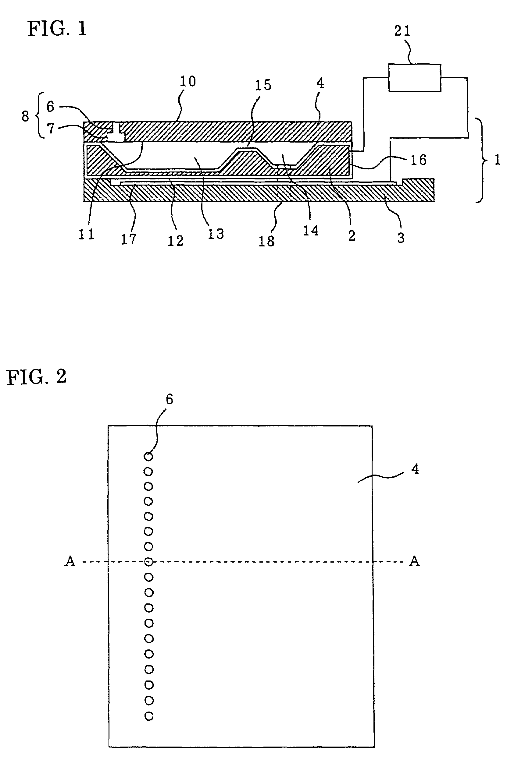
[0059]FIG. 1 is a vertical sectional view of a droplet ejection head according to a first embodiment of the present invention, in which a driving circuit 21 is shown schematically. The droplet ejection head shown in FIG. 1 is an example of an electrostatic droplet ejection apparatus of a face ejection type.

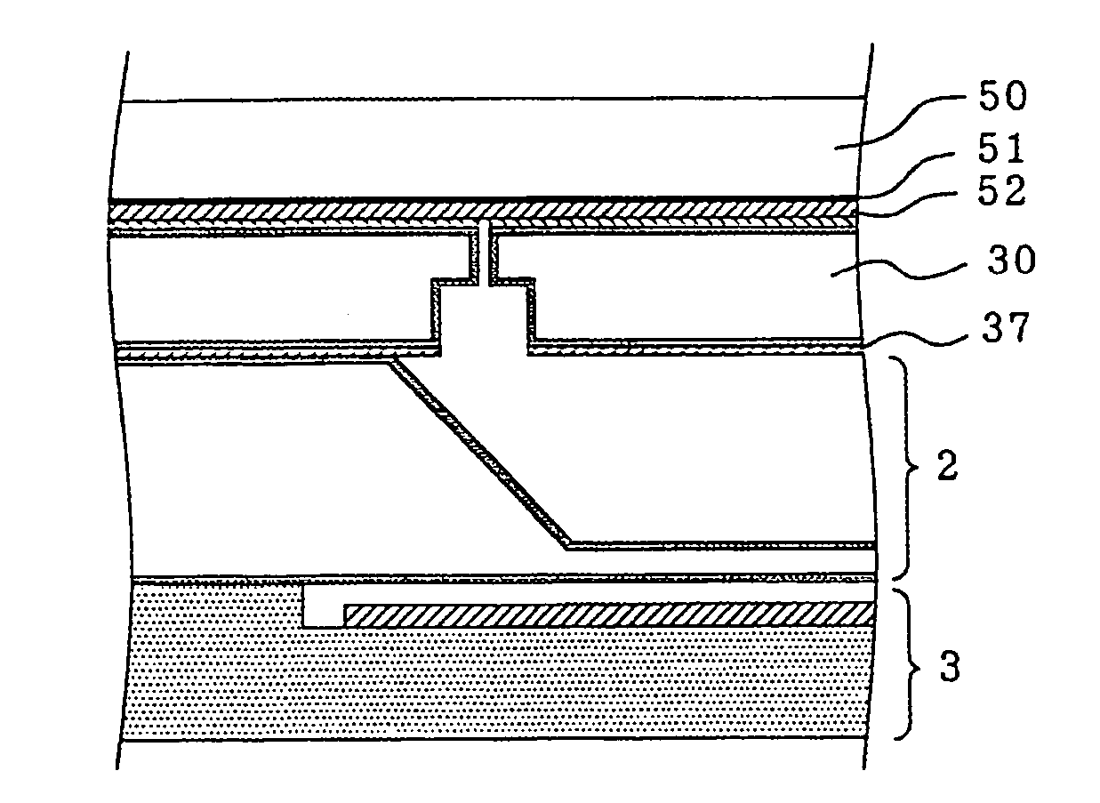
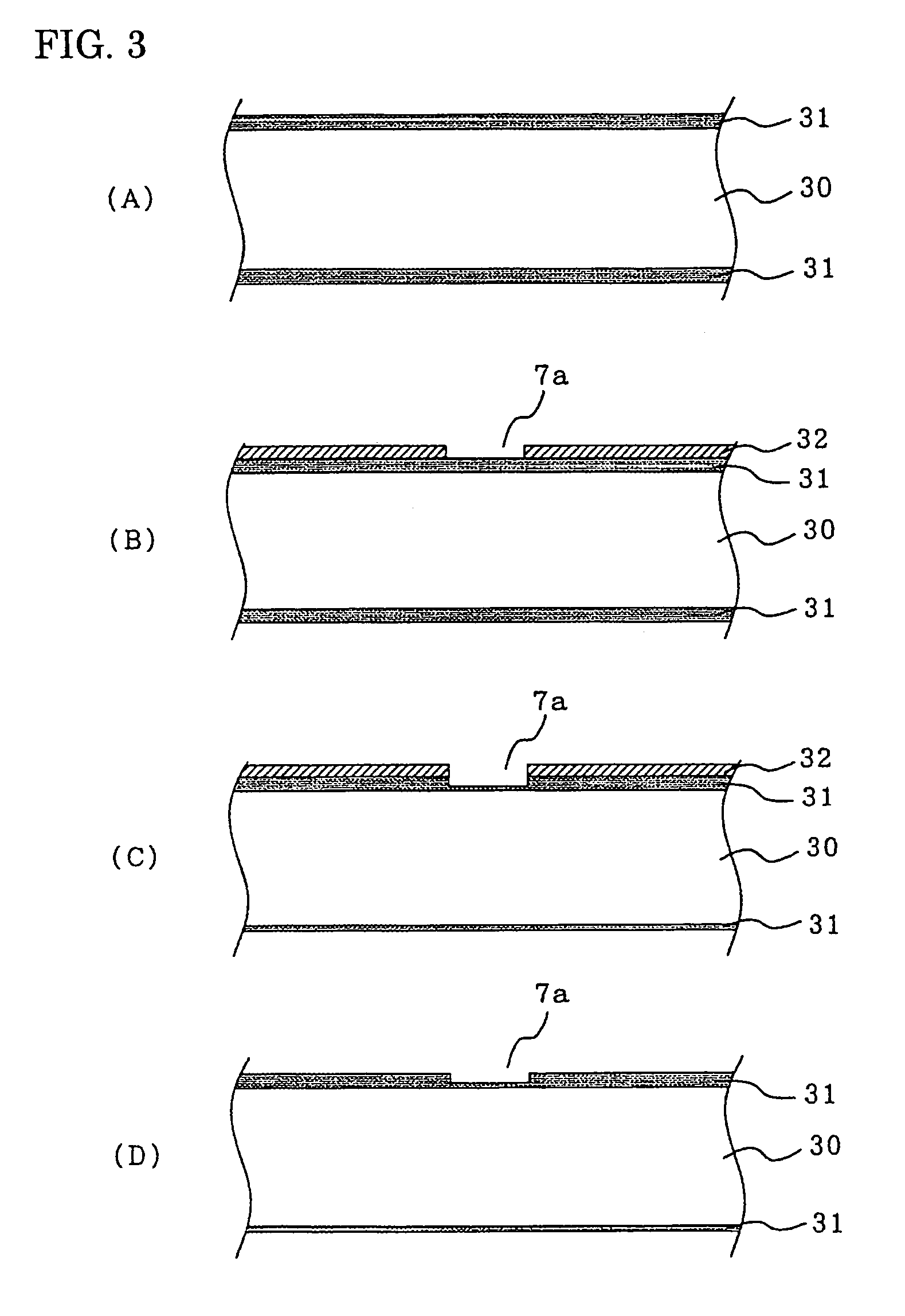
[0060]With reference to FIG. 1, reference numeral 1 represents the droplet ejection head. The droplet ejection head 1 principally includes a cavity substrate 2, an electrode substrate 3, and a nozzle substrate 4. The electrode substrate 3 and the nozzle substrate 4 are bonded to the cavity substrate 2. The nozzle substrate 4 is made of silicon and has nozzles 8 each having corresponding first nozzle channels 6 and second nozzle channels 7, connected to the first nozzle channels 6, having a diameter greater than that of the first nozzle channels 6. The first and second nozzle channels 6 and 7 have, for example, a cylindrical shape. The nozzle substrate 4 has a droplet ejection face...

second embodiment

[0115]FIG. 10 is a perspective view of an exemplary droplet ejection apparatus 100 including a droplet ejection head 1 manufactured by the method according to the first embodiment. The droplet ejection apparatus 100 shown in FIG. 10 is an ordinary inkjet printer.

[0116]The droplet ejection head 1 has no cracks or defects; hence, the droplet ejection apparatus 100 has high ejection performance.

[0117]The droplet ejection head 1 can be used for various applications, other than the inkjet printer, such as the manufacture of color filters for liquid crystal displays, the preparation of light-emitting sections of organic electroluminescent display systems, and the ejection of bioliquid by changing the type of liquid ejected from the droplet ejection head 1.

[0118]The droplet ejection head 1 can be used for piezoelectric droplet ejection apparatuses or bubble jet® type droplet ejection apparatuses.

[0119]A method for manufacturing a droplet ejection head, droplet ejection head, and droplet ej...


PUM

PropertyMeasurementUnit
thicknessaaaaaaaaaa
depthaaaaaaaaaa
depthaaaaaaaaaa

Abstract

A method for manufacturing a droplet ejection head includes a step of forming recessed sections for forming nozzles by etching half way through a first face of a silicon substrate, a step of bonding a first support substrate to the first face of the silicon substrate, a step of reducing the thickness of the silicon substrate by processing a second face of the silicon substrate that is opposite to the first face thereof, and making the recessed sections through holes, and a step of removing the first support substrate from the silicon substrate after the reduction of the thickness of the silicon substrate.

Description

[0001]The entire disclosure of Japanese Patent Application No. 2004-354989, filed Dec. 8, 2004, is expressly incorporated by reference herein.BACKGROUND OF THE INVENTION[0002]1. Field of the Invention[0003]The present invention relates to methods for manufacturing droplet ejection heads, droplet ejection heads, and droplet ejection apparatuses. The present invention particularly relates to a method for manufacturing a droplet ejection head having high ejection performance with high yield, a droplet ejection head manufactured by the method, and a droplet ejection apparatus including the droplet ejection head.[0004]2. Description of the Related Art[0005]Inkjet recording apparatuses have many advantages: high-speed printing, low noise during printing, great freedom in the selection of ink, and the use of inexpensive plain paper. Among such inkjet recording apparatuses, the following apparatus has recently become mainstream: an ink-on-demand type inkjet recording apparatus for ejecting ...

Claims


Application Information

Patent Timeline
Patent Type & Authority Patents(United States)
IPC IPC(8): B21D53/00
CPCB41J2/16B41J2/1623B41J2/1628B41J2/1634B41J2/1642B41J2/1646B41J2/1645Y10T29/49401B41J2002/043Y10T29/42Y10T156/1056B41J2/1621
Inventor ARAKAWA, KATSUJIMATSUMOTO, YASUTAKA
Owner SEIKO EPSON CORP
Why Eureka
Try Eureka