High performance multi-chip flip chip package

a multi-chip flip chip, high-performance technology, applied in the direction of semiconductor/solid-state device details, soldering apparatus, manufacturing tools, etc., can solve the problems of less than a performance limiting factor, poor heat dissipation, and inability to easily connect to the back side of the die, so as to reduce the resistance of the package to a negligible level, facilitate direct connection of the active surface of the silicon die to the printed circuit board, and improve the effect of thermal performan

Inactive Publication Date: 2009-05-26
SEMICON COMPONENTS IND LLC
View PDF45 Cites 9 Cited by
  • Summary
  • Abstract
  • Description
  • Claims
  • Application Information

AI Technical Summary

Benefits of technology

[0008]The present invention provides an improved multi-chip flip chip package that provides electrically isolated substrates, reduces package resistance to a negligible level, and offers superior thermal performance. Broadly, according to the present invention, a multi-chip carrier is provided that is made up of a first base layer separated from a second leadframe layer by a non-conductive laminating medium. The second leadframe layer is etched to form electrically isolated cavities to receive separate silicon dies. A silicon die is attached inside each cavity which is designed to surround the die along one or more edges of the die. Direct connection of the active surface of the silicon die to the printed circuit board is facilitated by an array of solder bumps that is distributed across the surface of each die as well as the edges of the leadframe layer surrounding each die. In one embodiment where connection to the back side of each die is required, the outer array of solder balls provide for low resistance electrical connection to the backside of each die that is attached to the leadframe layer. In applications where no connection to the back side of the die is required, the leadframe layer and the array of solder balls connecting to it may act as a thermal via for dissipating heat. Alternatively, the leadframe layer may be of dielectric material with selective conductive traces to make selective contact to traces on the board through the outer array of solder balls.
[0009]The multi-chip package of the present invention also reduces the number of steps required in the assembly process flow and is manufactured using standard materials and equipment. The resulting multi-chip package exhibits minimal resistance, improved heat dissipation, and is very thin and light as well as being cost-effective to manufacture. Furthermore, because of its construction, the multi-chip package of the present invention is able to withstand higher mechanical stress. It therefore enjoys improved reliability without the need for underfill that would otherwise be required for stress relief. Since each die would thus be essentially unencapsulated, the package may be rated at higher maximum junction temperatures, allowing for yet higher heat dissipation.

Problems solved by technology

Advances in semiconductor processing technology, however, have made the parasitics associated with conventional packages more of a performance limiting factor.
Because of poor heat dissipation from the laminated board, external heat sinks and additional PCB copper layers are often required to dissipate excess heat.
In the case of conventional flip chip technology, among other shortcomings, heat dissipation is essentially governed by the die size and connection to the back side of the die is not easily facilitated (often requiring a bond wire connection).
These limitations—poor heat dissipation and resistive contact to back side—become quite significant in high current applications such as power switching devices.
This package exhibits significantly lower resistance; however, it still relies on a lead frame which adds residual resistance to the current path, and is not the smallest package possible for a given die size.
The drawbacks associated with using flip chip interconnection in high current applications continue to persist in the MCM environment.
The conventional MCM packaging introduces an additional problem in that the substrate upon which the multiple dies are mounted is common to all of the individual dies.
An electrically common substrate severely limits the range of applications for the flip chip-connected MCM device.
An MCM carrier with an electrically common substrate, therefore, would not allow packaging of MOSFETs that require separate drain connections.

Method used


Image

  • High performance multi-chip flip chip package
  • High performance multi-chip flip chip package
  • High performance multi-chip flip chip package

Examples


Embodiment Construction

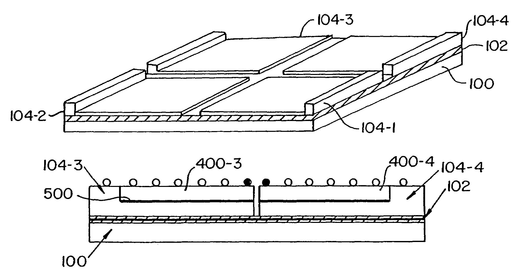
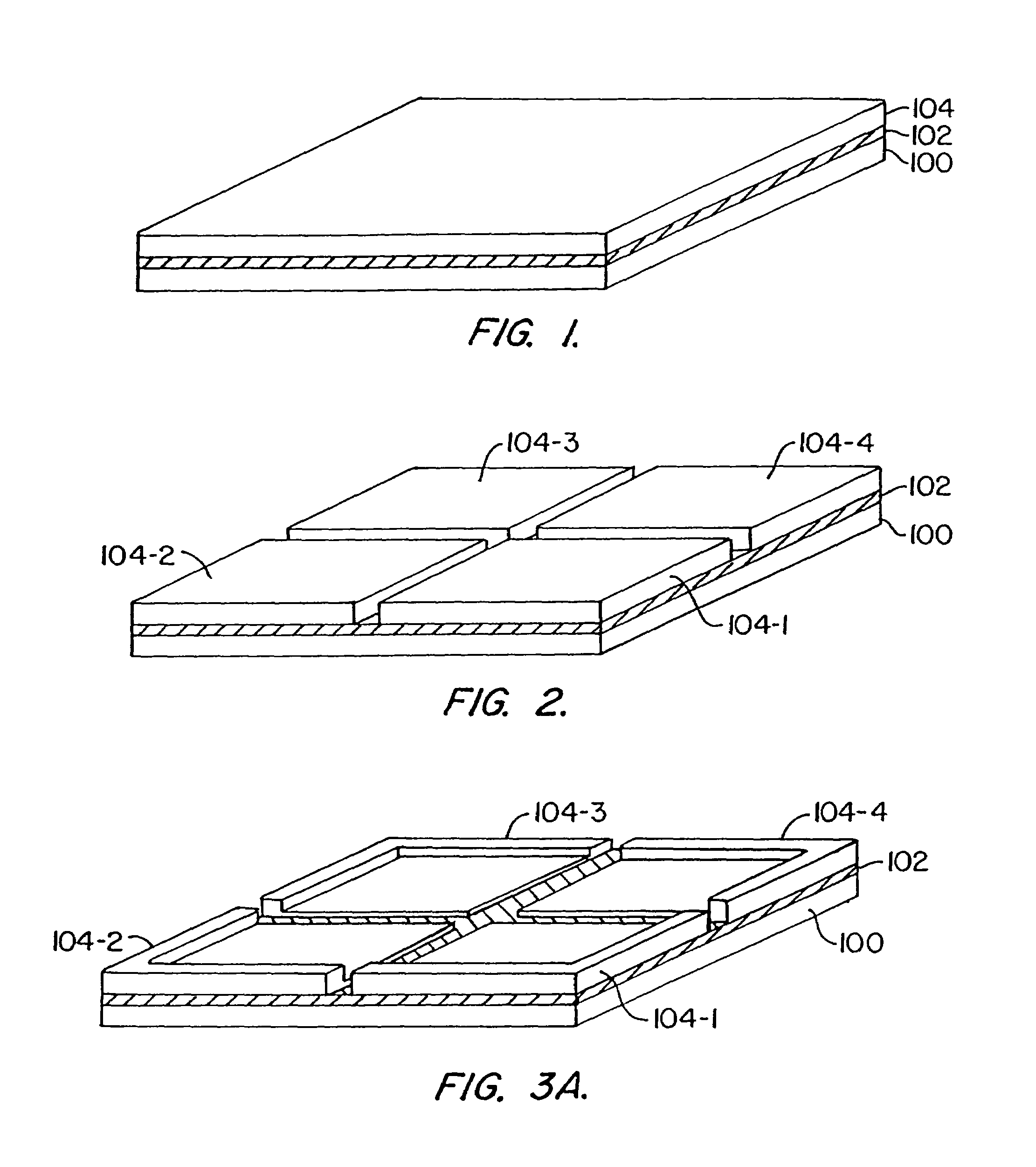
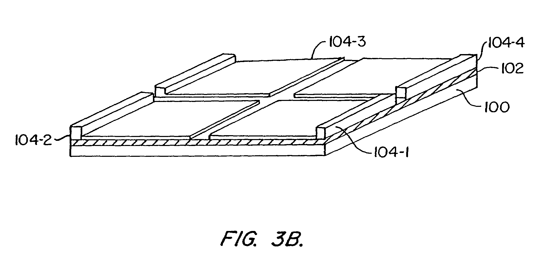
[0021]An improved flip chip packaging technology that offers a number of advantages over conventional semiconductor packaging technologies is described in detail in the above-referenced parent application Ser. No. 09 / 129,663, by R. Joshi. Briefly, according to the improved flip chip technology, a silicon die is attached to a carrier (or substrate) that has a cavity substantially surrounding the die. Direct connection of the active surface of the silicon die to the printed circuit board is then made by an array of solder bumps that is distributed across the surface of the die as well as the edges of the carrier surrounding the die. This eliminates the use of wire bonds or extended lead frames and results in a package that exhibits substantially reduced resistance and superior thermal performance. If the substrate is made large enough, the same manufacturing process can be used to house multiple dies inside one package. There would be one restriction however: with a common substrate, ...


PUM

PropertyMeasurementUnit
sizeaaaaaaaaaa
thicknessaaaaaaaaaa
conductiveaaaaaaaaaa

Abstract

A structure and method of manufacture for an improved multi-chip semiconductor package that reduces package resistance to a negligible level, and offers superior thermal performance. Housing of multiple dies is facilitated by providing electrically isolated lead frames that are separated from a common base carrier by a non-conductive layer of laminating material. A silicon die is attached inside a cavity formed in each lead frame. Direct connection of the active surface of the silicon die to the printed circuit board is then made by an array of solder bumps that is distributed across the surface of each die as well as the edges of the lead frame adjacent to each die.

Description

CROSS-REFERENCE TO RELATED APPLICATIONS[0001]This application is a continuation application of U.S. patent application Ser. No. 10 / 741,217, filed on Dec. 19, 2003, which is a continuation of U.S. patent application Ser. No. 10 / 309,661, filed on Dec. 3, 2002, now U.S. Pat. No. 6,696,321, which is a divisional of U.S. patent application Ser. No. 09 / 285,191, filed on Mar. 15, 1999, now U.S. Pat. No. 6,489,678, which is a continuation-in-part of U.S. patent application Ser. No. 09 / 129,663, filed Aug. 5, 1998, entitled “High Performance Flip Chip Package,” now U.S. Pat. No. 6,133,634, the disclosures of which are all incorporated herein by reference.BACKGROUND OF THE INVENTION[0002]The present invention relates in general to semiconductor packaging and in particular to an apparatus and method of manufacture for a multi-chip high performance flip chip package for semiconductor devices.[0003]While silicon process technology has advanced significantly in the past decade, for the most part, ...

Claims


Application Information

Patent Timeline
Patent Type & Authority Patents(United States)
IPC IPC(8): H01L21/44H01L21/48H01L21/50B23K1/00B23K3/06H01L23/492
CPCB23K1/0008B23K3/0623H01L23/492B23K2201/40H01L2924/0002H01L2924/00B23K2101/40
Inventor JOSHI, RAJEEV
Owner SEMICON COMPONENTS IND LLC
Why Eureka
Try Eureka