Integrated lateral mode converter

a technology of integrated circuits and lateral modes, applied in the field of optical integrated circuits based on photonic integrated circuits, can solve the problems of cost barriers, lowering the overall cost of ownership, and continuing downward pressure on the core optoelectronic componentry

Active Publication Date: 2009-05-26
ONECHIP PHOTONICS
View PDF6 Cites 68 Cited by
  • Summary
  • Abstract
  • Description
  • Claims
  • Application Information

AI Technical Summary

Benefits of technology

[0015]In accordance with the invention, integrated mode converter is designed to be used in the devices in which light generation occurs in one of the higher-order mode. Additionally, it is assumed that light generation is taking place in one of the active waveguides incorporated in a multi-layered semiconductor structure. The invention relies on using cascaded resonance coupling between the waveguides formed both in the vertical and lateral directions with reference to the multi-layered semiconductor structure. The invention discloses transforming a higher-order mode generated in the active waveguide into the fundamental zero-order mode of the passive waveguide for successive coupling into an optical fiber or into other optical component.
[0016]In an illustrative embodiment, a monolithically integrated device has a first waveguide which is an active waveguide and where higher-order mode is generated and a second waveguide which is a passive waveguide and which is vertically adjacent to the first waveguide and to which higher order mode from the active waveguide is transferred without changing its symmetry. Laterally adjacent to the second waveguide is a third waveguide which has geometrical characteristics (ridge width) different from those of the second waveguide and to which light from the second waveguide is transferred and where field profile takes the form of the fundamental mode.
[0017]A mode transformer embodying in the invention may be employed in conjunction with both the distributed feedback and the Fabry-Perot-type laser diodes. In the latter case the mode transformer being a part of laser cavity fulfills stabilizing function for the particular higher-order mode generated by the laser. Namely, because the mode transformer operates in a manner of a filter which provides minimal transmission loss for the mode of particular order, this particular higher-order mode has preference to be generated as compared to other higher-order modes.

Problems solved by technology

Such economic drivers including lowering overall cost-of-ownership, increased services and service delivery, and resulting in continued downward pressure on the core optoelectronic componentry.
However, even such monolithic integration can provide cost barriers with poor design methodologies, low manufacturing yields, complicated manufacturing processes and repeated expensive epitaxial growth processes.
Providing optical coupling from one layer to another, as well as controlling the spatial field profile of propagating optical signals are inevitable challenges in the PIC design.
However, whilst efficient and stable optical generation is achieved in the first or in other higher-order mode, the challenge is then an efficient transfer of the optical signal from the spatial profile of the higher-order mode into the fundamental mode of an optical fiber or another photonic component.
Another limitation of the invention is that it converts an initial transverse electric (TE) zero-order mode into a transverse magnetic (TM) first-order mode as is disclosed in the patent, conversion of the mode of higher order being taught as problematic.
Namely, an enormous difficulty related to the light coupling from one chip to another and high insertion loss associated with such coupling rules out application of the prior art by Kazarinov in the monolithic integration architecture.
Namely, sophisticated electrical circuitry and packaging, device calibration and re-calibration when external conditions change, and an overall increase in both device production and operation costs.
While the suggested approach can be readily used for monolithic integration of the mode converter into a photonic chip, demonstrated performance of conversion efficiency is low and not compatible with the constraints of an optical power budget within the PIC to meet commercial OLT specifications at neither low cost nor optical crosstalk requirements between the multiple elements of the PIC.

Method used


Image

  • Integrated lateral mode converter
  • Integrated lateral mode converter
  • Integrated lateral mode converter

Examples


Embodiment Construction

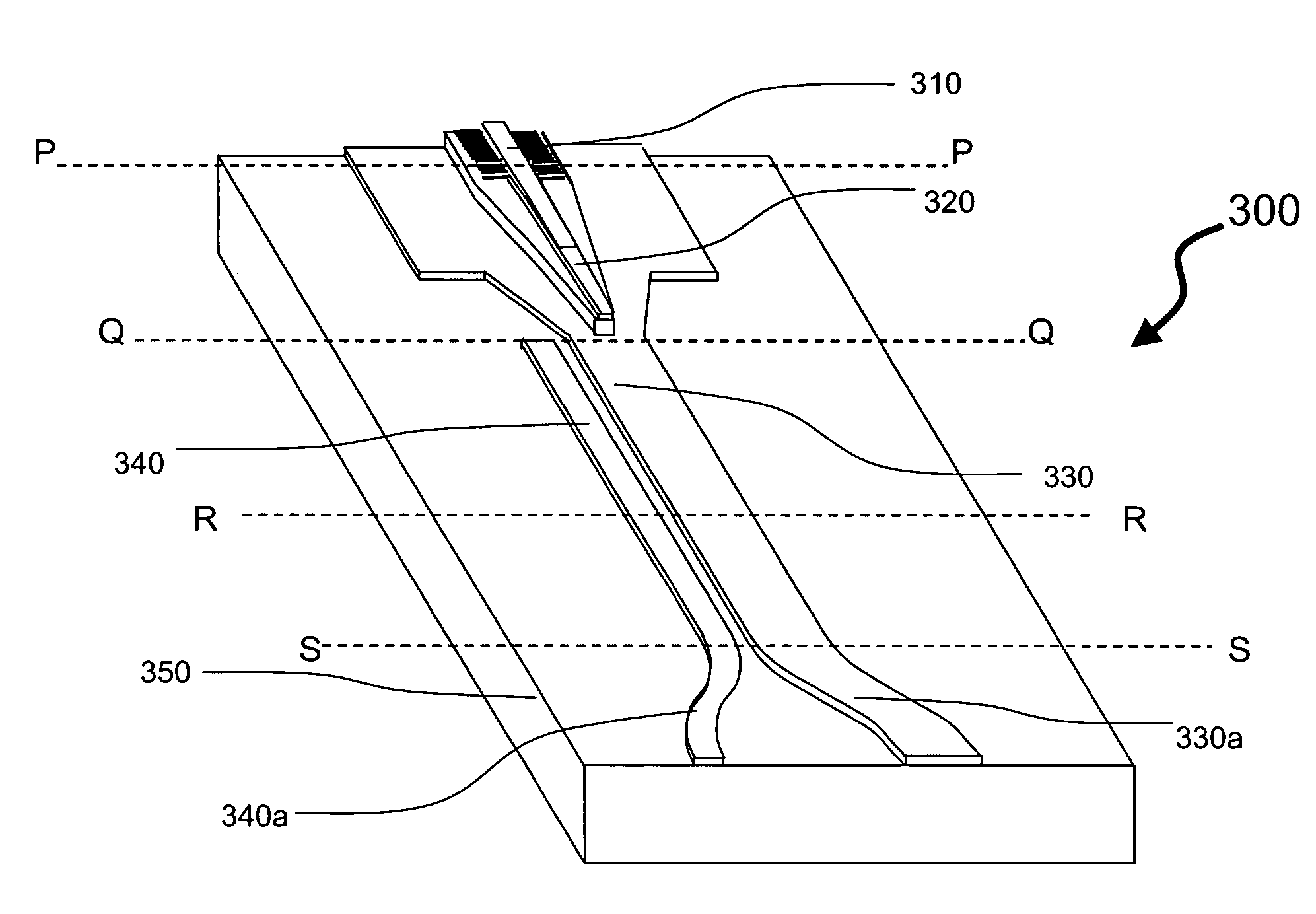
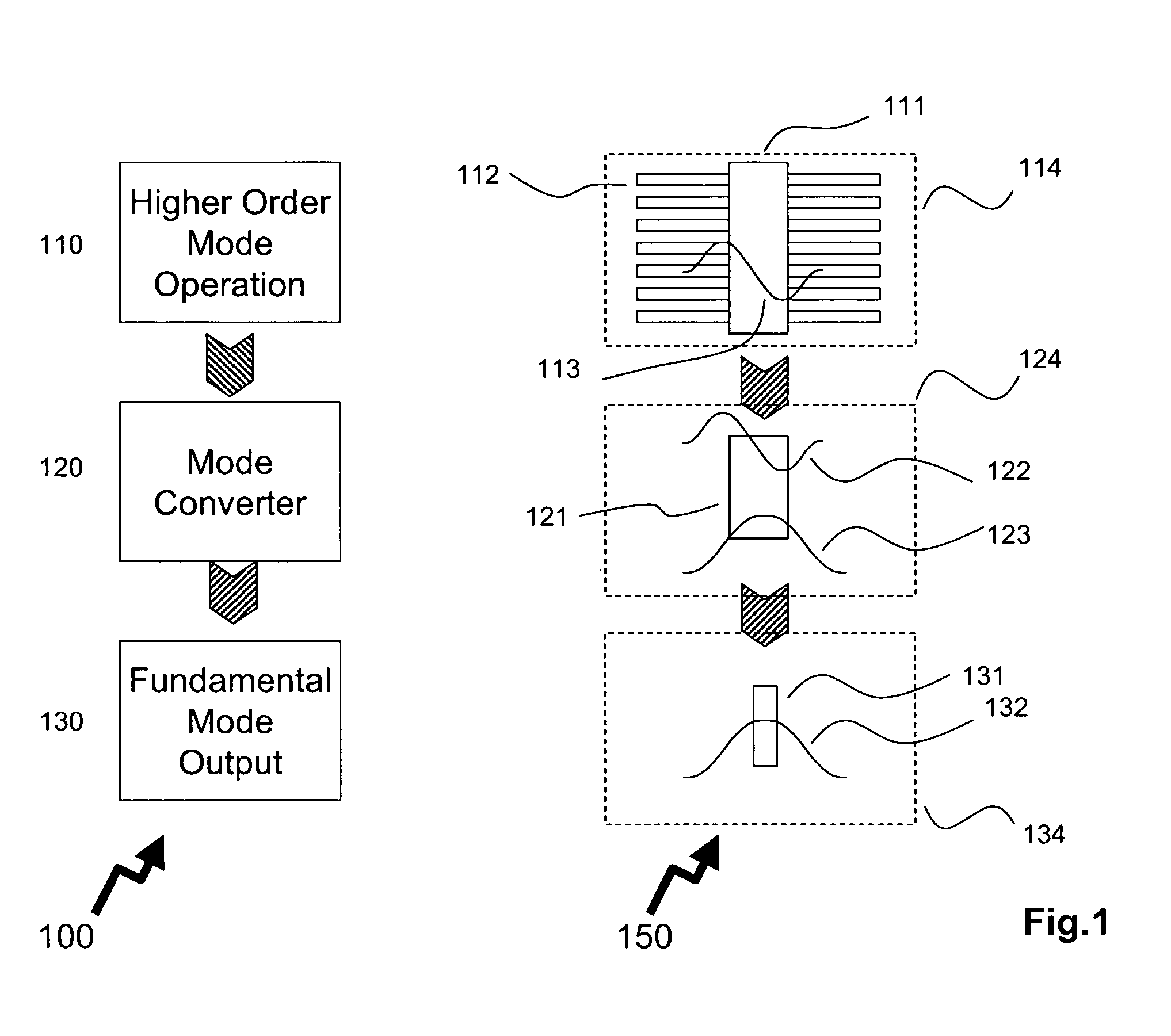
[0026]Referring to FIG. 1 a mode converter is schematically shown as a flow diagram 100 wherein an optical element operates in a higher order mode of operation 110 which should be coupled to a fundamental mode output 130 for satisfactory coupling to subsequent optical elements. Accordingly the flow diagram 100 shows an intermediate operation of a mode converter 120 providing this functional shift in operation of the overall optical assembly. Referring to schematic diagram 150 this flow diagram 100 is depicted schematically as discrete functional elements. Accordingly, the higher order mode of operation 110 is depicted by laser element 114 and consists of laser stripe 111 with grating structure 112 and operating in higher order mode 113.

[0027]This higher order mode 113 becomes input field 122 of modal converter 124, representing mode converter 120, which adiabatically couples for lowest insertion loss to a first fundamental mode 123 of the modal converter 124. This first fundamental ...


PUM


Abstract

The invention describes method and apparatus for a mode converter enabling an adiabatic transfer of a higher order mode into a lower order optical mode within a photonic integrated circuit exploiting integrated semiconductor ridge waveguide techniques. As disclosed by the invention, such a mode conversion is achievable by using an asymmetric coupler methodology. In an exemplary embodiment of the invention, the invention is used to provide a low insertion loss optical connection between laterally-coupled DFB laser operating in first order mode and passive waveguide operating in the zero order optical mode. The integrated arrangement fabricated by using one-step epitaxial growth allows for a launch of the laser's light into the waveguide circuitry operating in the zero order lateral mode or efficiently coupling it to single-mode fiber, an otherwise high loss interface due to the difference in laser and optical fiber modes.

Description

FIELD OF THE INVENTION[0001]The invention relates to optical waveguides and more particularly to a photonic integrated circuit based optical field profile transformer for converting higher-order modes into a fundamental zero-order mode of the waveguide.BACKGROUND OF THE INVENTION[0002]Modern telecommunication technologies based on optical fibers and associated optoelectronic components are designed to deliver a variety of advanced services ranging from ultra-long distance submarine transmission, to very high capacity 10 Gbs and 40 Gb / s long-haul terrestrial backbone, through Metropolitan Area Networks (MANs) and access networks such as the “triple play” subscriber access of plain-old-telephone-service (POTS), broadband Internet, and television. The penetration of such “triple-play” service by provision of optical access networks with projected subscriber terminations requiring massive quantities of optical line terminal (OLT) equipment is strongly driven by the operators and service...

Claims


Application Information

Patent Timeline
Patent Type & Authority Patents(United States)
IPC IPC(8): G02B6/26
CPCG02B6/12004G02B6/131G02B6/14
Inventor LOGVIN, YURYWU, FANGPIMENOV, KIRILLTOLSTIKHIN, VALERY
Owner ONECHIP PHOTONICS
Why Eureka
Try Eureka