
Formation of carbon and semiconductor nanomaterials using molecular assemblies

a technology of molecular assemblies and nanomaterials, which is applied in the direction of nanoinformatics, polycrystalline material growth, crystal growth process, etc., can solve the problems of limited success in the formation of electrical devices using carbon nanotubes, small portion of individual nanotubes actually coming into contact with electrodes, and nanostructures to potentially harmful conditions. , to achieve the effect of increasing the amount of metal on the surfa

Active Publication Date: 2009-06-09
GLOBALFOUNDRIES U S INC
View PDF8 Cites 16 Cited by
  • Summary
  • Abstract
  • Description
  • Claims
  • Application Information

AI Technical Summary

Benefits of technology

[0034]The inventive process can provide several advantages over the making of electronic devices. Some of these advantages include:

Problems solved by technology

Once harvested, one remaining challenge is to position the carbon nanomaterials for use in devices, e.g., positioning them between electrodes on selected substrates for electronic, optoelectronic or sensing applications.
However, only a small portion of the individual nanotubes actually come in contact with the electrodes.
The successful formation of electrical devices using carbon nanotubes is limited by serendipitous electrode patterning or random nanotube deposition or if the electrodes are intentionally aligned to the nanotubes, to small numbers of devices.
At the research level the attractive performance of carbon nanotubes in electronics and optoelectronics has been demonstrated, however, challenges remain with regard to scale-up of carbon nanotube device application and, in particular, in providing reliable contacts between the nanotubes and the electrodes of the device.
Again, the process of harvesting and positioning nanowires on surfaces subjects the nanostructures to potentially harmful conditions.
Although this approach may eliminate the need to harvest and place the nanotubes or nanowires in some applications, vertical arrays of these materials place severe constraints on device geometries and assumes that the growth surface is amenable to the desired device structure.
Lithographic patterning of surfaces is useful across the substrate plane, but does not provide a route to pattern surfaces vertically.

Method used


Image

  • Formation of carbon and semiconductor nanomaterials using molecular assemblies
  • Formation of carbon and semiconductor nanomaterials using molecular assemblies
  • Formation of carbon and semiconductor nanomaterials using molecular assemblies

Examples


example 1

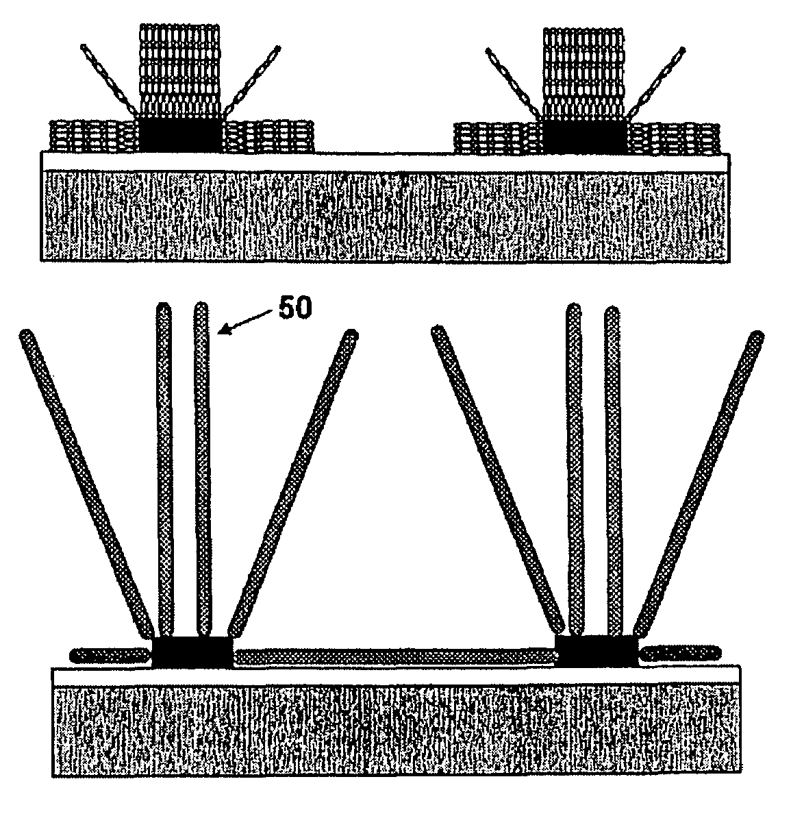
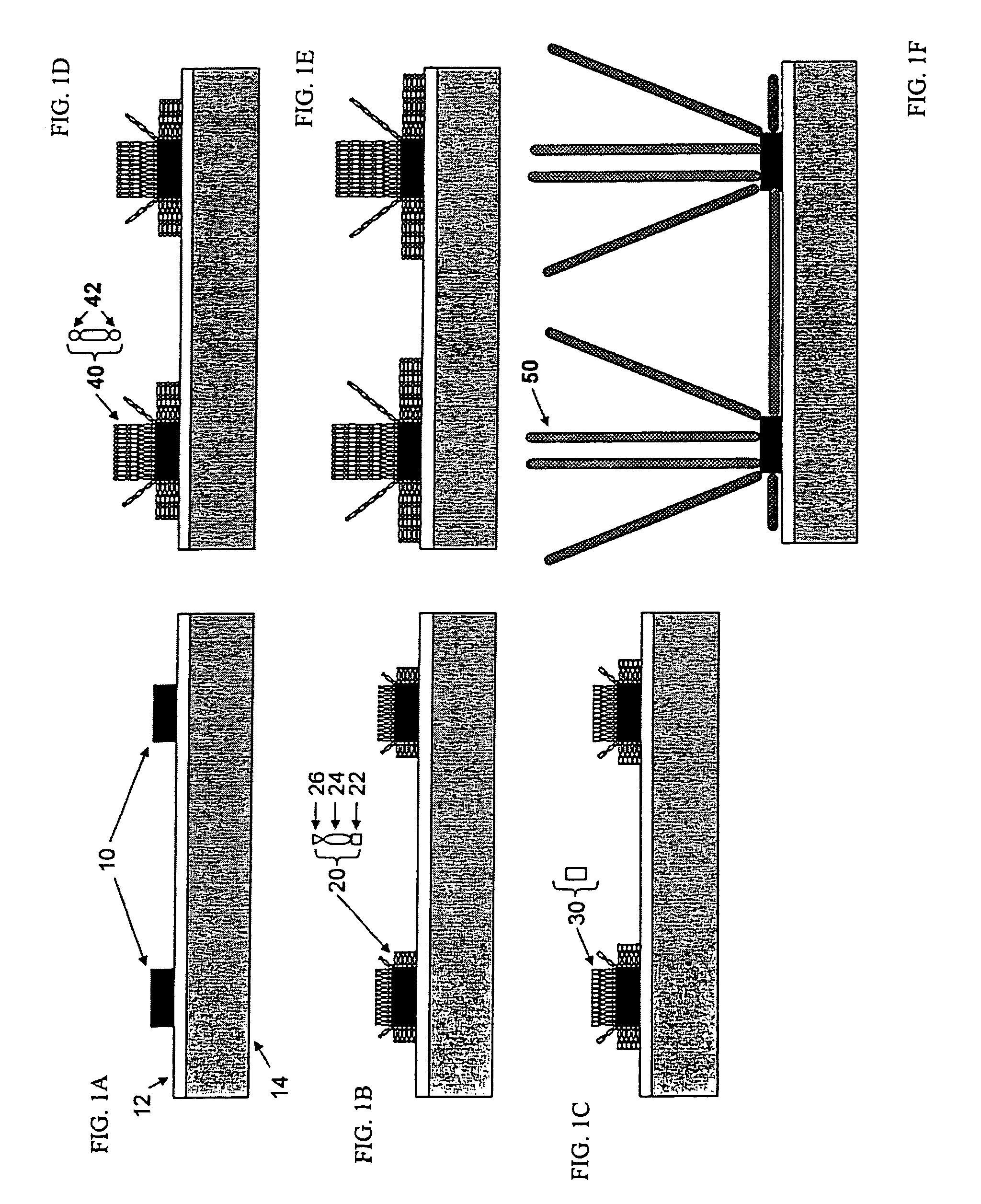
[0079]A heavily n+ doped silicon wafer, with 10 nm thermally grown silicon oxide was patterned with electrodes consisting of 10 Å Ti followed by 190 Å Pd. The patterned substrate was exposed to 1 mM mercaptoterypyridine in 50:50 toluene:ethanol for a period of 18 hrs, resulting in the assembly of mercaptoterypridine on the Pd surfaces. The samples were rinsed well in clean 50:50 toluene:ethanol and exposed to 5 mM Fecl3 in ethanol for a similar period of 18 hrs. The samples were rinsed in clean ethanol and dried under a nitrogen stream.

example 2

[0080]A heavily n+ doped silicon wafer, with 10 nm thermally grown silicon oxide was patterned with electrodes consisting of 10 Å Ti followed by 190 Å Pd. The patterned substrate was exposed to 1 mM mercaptoterypyridine in 50:50 toluene:ethanol for a period of 18 hrs, resulting in the assembly of mercaptoterypridine on the Pd surfaces. The samples were rinsed well in clean 50:50 toluene:ethanol and exposed to dispersion of iron oxide nanoparticles in hexane for a period of 18 hrs. The samples were rinsed in clean hexane and dried under a nitrogen stream.

example 3

[0081]A heavily n+ doped silicon wafer, with 10 nm thermally grown silicon oxide was patterned with electrodes consisting of 10 Å Ti followed by 190 Å Pd. The patterned substrate was exposed to 1 mM aminoethanethiol in ethanol for 18 hrs, resulting in the assembly of aminoethanethiol on the Pd surfaces. The samples were rinsed well with clean ethanol and exposed to a dispersion of iron oxide nanoparticles in hexane for a period of 18 hrs. The samples were rinsed in clean hexane and dried under a nitrogen stream.


PUM

PropertyMeasurementUnit
depositionaaaaaaaaaa
electric fieldsaaaaaaaaaa
polarizabilityaaaaaaaaaa

Abstract

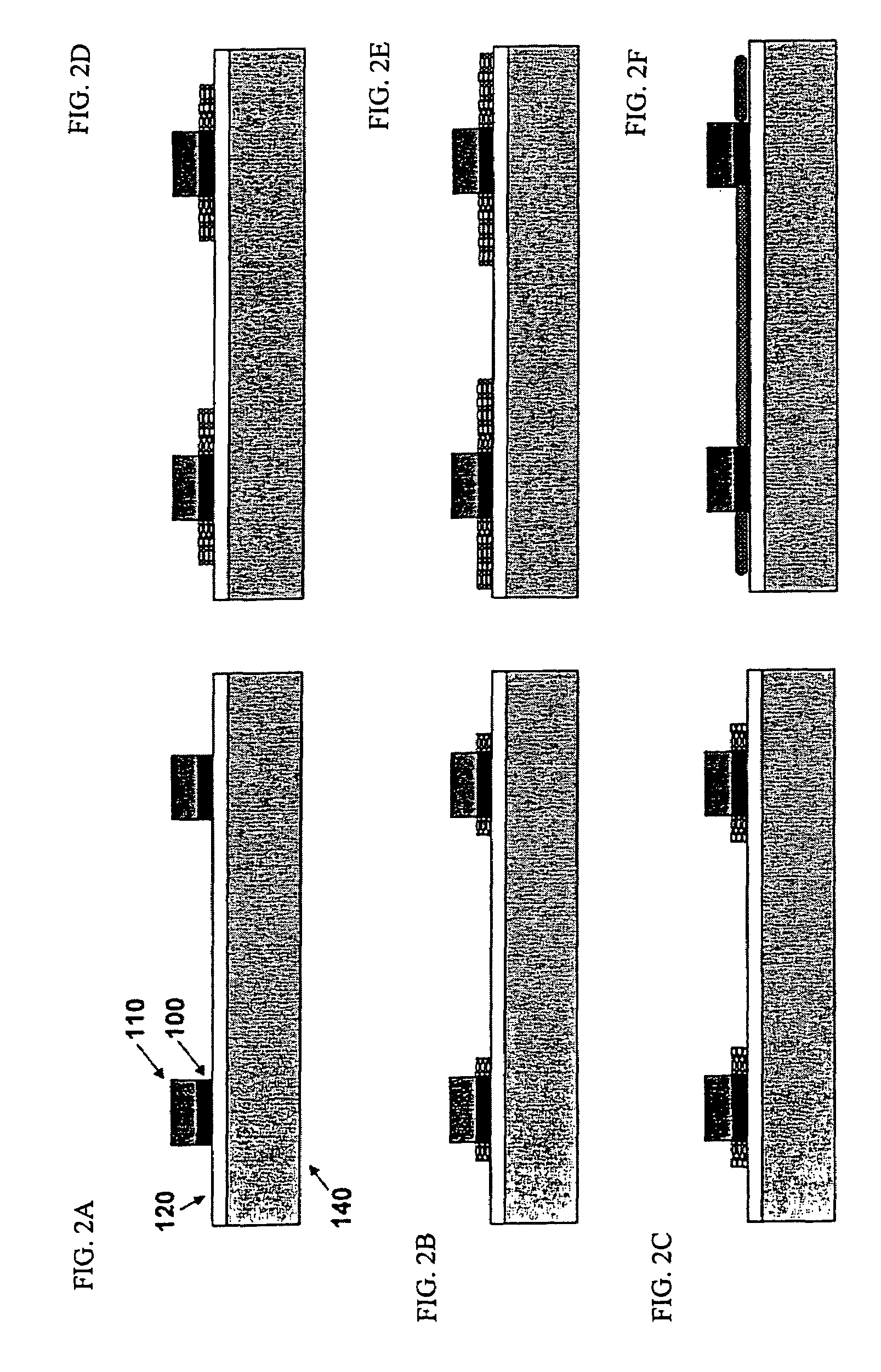
The invention is directed to a method of forming carbon nanomaterials or semiconductor nanomaterials. The method comprises providing a substrate and attaching a molecular precursor to the substrate. The molecular precursor includes a surface binding group for attachment to the substrate and a binding group for attachment of metal-containing species. The metal-containing species is selected from a metal cation, metal compound, or metal or metal-oxide nanoparticle to form a metallized molecular precursor. The metallized molecular precursor is then subjected to a heat treatment to provide a catalytic site from which the carbon nanomaterials or semiconductor nanomaterials form. The heating of the metallized molecular precursor is conducted under conditions suitable for chemical vapor deposition of the carbon nanomaterials or semiconductor nanomaterials.

Description

FIELD OF THE INVENTION[0001]This invention relates to the use of molecular assemblies to direct the formation of carbon nanomaterials and semiconductor nanomaterials. The invention also relates to electronic and optoelectronic devices made with carbon and semiconductor nanomaterials formed using the molecular assemblies.BACKGROUND OF THE INVENTION[0002]Carbon nanotubes, which can be either semiconducting or metallic, are typically grown by arc discharge, laser ablation, or chemical vapor deposition. The nanotubes are then harvested from the growth surface for subsequent use [H. Dai, Acc. Chem. Res. 35, 1035 (2002)]. Once harvested, one remaining challenge is to position the carbon nanomaterials for use in devices, e.g., positioning them between electrodes on selected substrates for electronic, optoelectronic or sensing applications. At the research level, individual carbon nanotubes are commonly brought into contact with electrodes by one of two techniques. In one instance, the carb...

Claims


Application Information

Patent Timeline
Patent Type & Authority Patents(United States)
IPC IPC(8): B82B1/00B82B3/00
CPCB82Y10/00B82Y30/00B82Y40/00C01B31/0233C30B25/00C30B29/02C30B29/60H01L29/0665H01L29/0673H01L29/0676H01L29/78681H01L29/78684Y10S977/89Y10S977/762Y10S977/932Y10S977/84Y10S977/936Y10S977/938C01B32/162
Inventor AFZALI-ARDAKANI, ALIKAGAN, CHERIE R.KOSBAR, LAURA L.
Owner GLOBALFOUNDRIES U S INC
Learn More