
Light emitting element, light emitting device and semiconductor device

a technology of light emitting devices and light emitting elements, which is applied in the direction of solid-state devices, electric lighting sources, electric light sources, etc., can solve the problems of poor element quality, troublesome adjustment or the like of a material, and unsuitable coating performance, and achieve the effect of convenient manufacturing

Inactive Publication Date: 2009-06-23
SEMICON ENERGY LAB CO LTD
View PDF19 Cites 4 Cited by
  • Summary
  • Abstract
  • Description
  • Claims
  • Application Information

AI Technical Summary

Benefits of technology

[0009]It is an object of the present invention to provide a light emitting element which is easily manufactured with a wet method.
[0013]According to the invention, a light emitting element having a few poor elements due to failure of a layer formed by a wet method can be obtained. In addition, a light emitting device which can easily make ohmic contact between a wiring and an electrode of the light emitting element and further has little poor light emitting element due to failure of a layer formed by a wet method can be obtained.

Problems solved by technology

In the case of using an ink-jet method or a coating method as described above, coating is not suitably performed if an object to be treated has low wettability, which contributes to a poor element.
However, a method as in Patent Document 1 has trouble with the adjustment or the like of a material for forming the wettability changing layer.

Method used


Image

  • Light emitting element, light emitting device and semiconductor device
  • Light emitting element, light emitting device and semiconductor device
  • Light emitting element, light emitting device and semiconductor device

Examples


embodiment mode 1

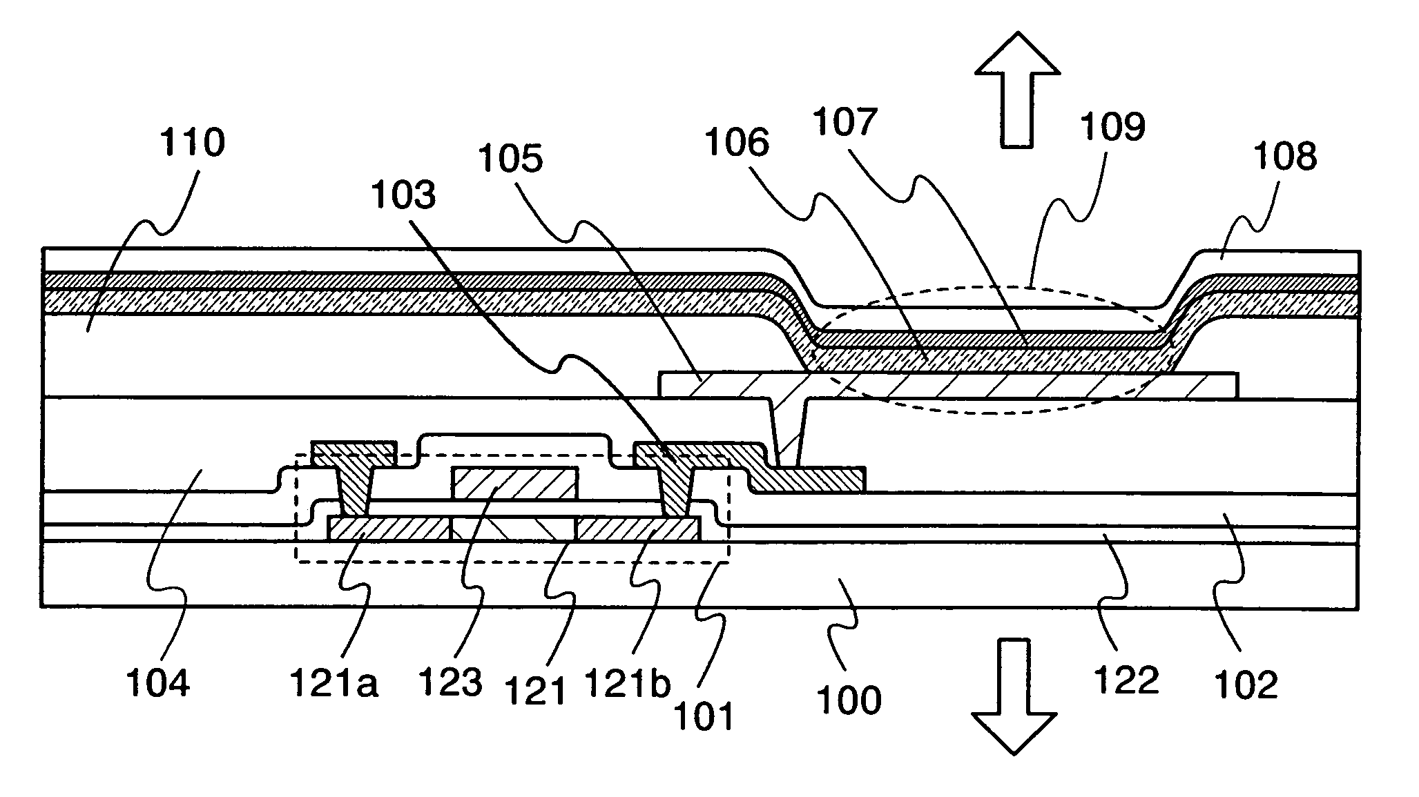
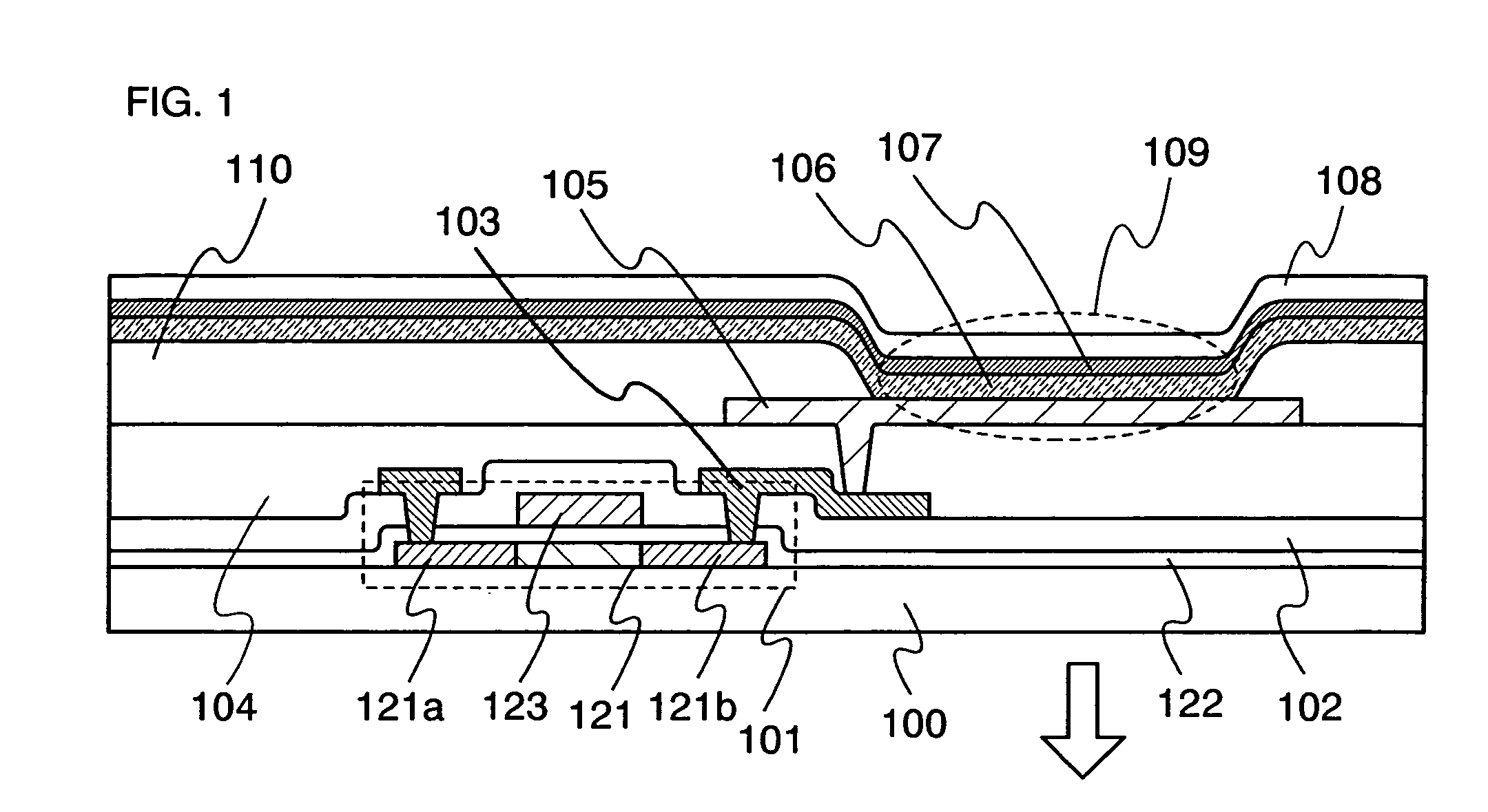
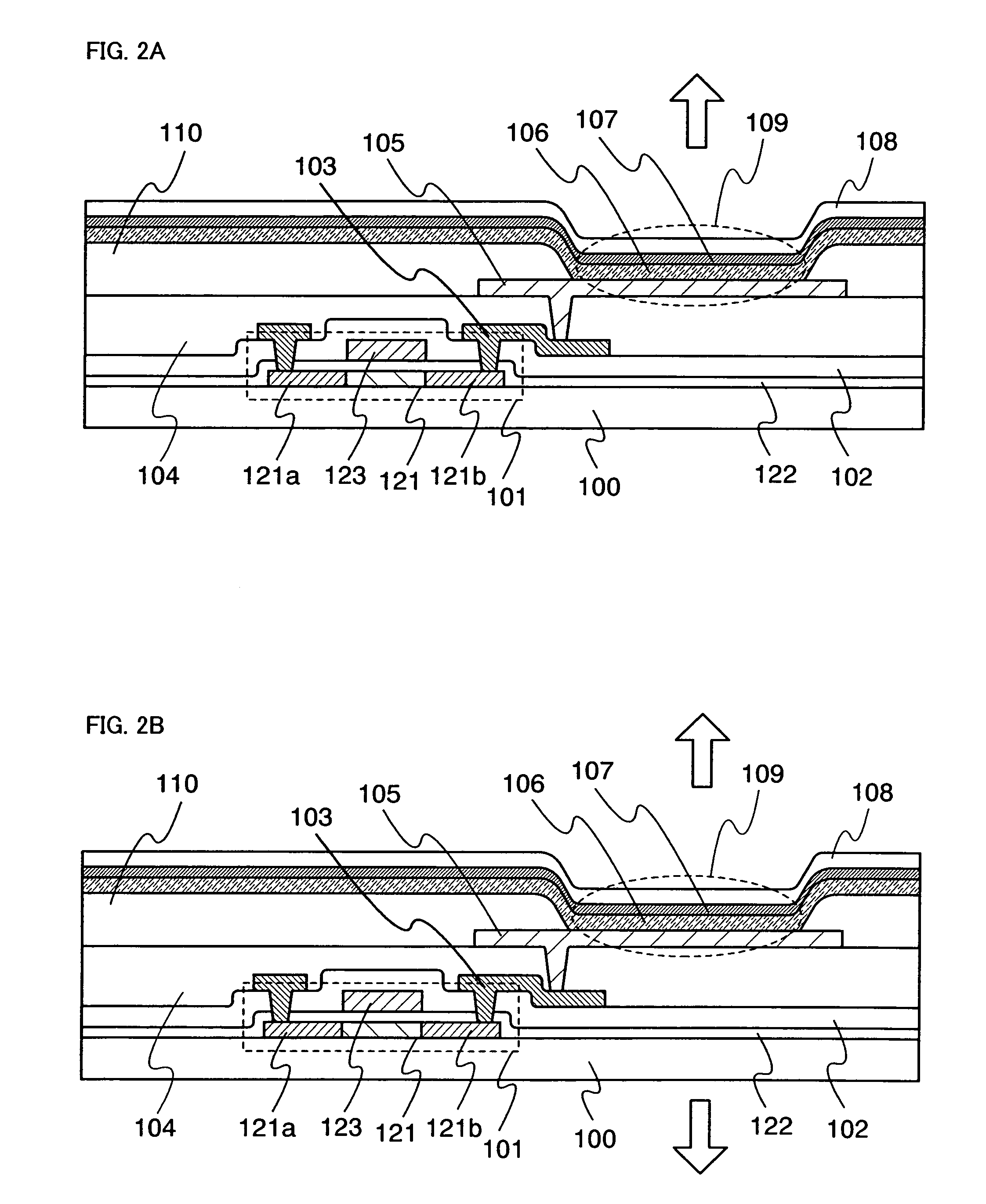
[0024]One mode of a light emitting device according to the invention is described with reference to FIG. 1.

[0025]A transistor 101 and the like are manufactured over a substrate 100. Here, the substrate 100 is not limited in particular, and a substrate having flexibility such as a plastic substrate as well as a glass substrate, a quartz substrate, or the like can be used. Further, the transistor 101 shown in FIG. 1 is a top-gate transistor in which a gate insulating layer 122 and a gate electrode 123 are sequentially formed over a semiconductor layer 121; however, the structure of a transistor is not limited in particular, and a bottom-gate transistor may be used as well as the top-gate transistor. Further, an element such as a capacitor element may be manufactured as well as a transistor. The semiconductor layer which is included in the transistor 101 may be a semi-amorphous layer or the like as well as a layer containing a crystalline component or a layer containing a non-crystalli...

embodiment mode 2

[0038]In this embodiment mode, a light emitting device according to the present invention including a bottom-gate transistor 201 is described with reference to FIGS. 3A and 3B.

[0039]In FIG. 3A, a gate electrode 221 is formed over a substrate 200, and a gate insulating layer 222 which covers the gate electrode 221 is further formed. A semiconductor layer 223 is further formed over a portion in which the gate insulating layer 222 overlaps the gate electrode 221. An N-type semiconductor layer 224 is formed over a region except a channel formation region in the semiconductor layer 223.

[0040]Thus, the bottom-gate transistor 201 including the gate electrode 221, the gate insulating layer 222, the semiconductor layer 223, and the N-type semiconductor layer 224 is electrically connected to a wiring 202 since the N-type semiconductor layer 224 is in contact with the wiring 202.

[0041]Further, similarly to the semiconductor layer 121 mentioned in Embodiment Mode 1, the semiconductor layer 224 ...

embodiment mode 3

[0052]In this embodiment mode, a circuit configuration and a driving method of a light emitting device having a display function, which is a light emitting device as described in Embodiment Mode 1, are described with reference to FIGS. 3A to 6.

[0053]FIG. 4 is a schematic top view of a light emitting device to which the present invention is applied. In FIG. 4, a pixel portion 6511, a source signal line driver circuit 6512, a writing gate signal line driver circuit 6513, and an erasing gate signal line driver circuit 6514 are provided over a substrate 6500. The source signal line driver circuit 6512, the writing gate signal line driver circuit 6513, and the erasing gate signal line driver circuit 6514 each are connected to an FPC (Flexible Printed Circuit) 6503 which is an external input terminal through a group of wirings. The source signal line driver circuit 6512, the writing gate signal line driver circuit 6513, and the erasing gate signal line driver circuit 6514 each receives a ...


PUM

PropertyMeasurementUnit
grain diameteraaaaaaaaaa
wavenumberaaaaaaaaaa
temperatureaaaaaaaaaa

Abstract

It is an object of the present invention to provide a semiconductor device, in particular, a light emitting element which can be easily manufactured with a wet method. One feature of the invention is a light emitting device including a transistor and a light emitting element. In the light emitting element, an organic layer, a light emitting layer, and a second electrode are sequentially formed over a first electrode, and the transistor is electrically connected to the light emitting element through a wiring. Here, the wiring contains aluminum, carbon, and titanium. The organic layer is formed by a wet method. The first electrode which is in contact with the organic layer is formed from indium tin oxide containing titanium oxide.

Description

BACKGROUND OF THE INVENTION[0001]1. Field of the Invention[0002]The present invention relates to a light emitting element having a light emitting layer between a pair of electrodes, a light emitting device including the light emitting element, and generally relates to other semiconductor devices.[0003]2. Description of the Related Art[0004]These days, most of light emitting elements utilized for a display or the like has a structure in which a light emitting layer is interposed between a pair of electrodes. In such the light emitting element, light is emitted when an exciton formed by recombining an electron injected from one of the electrodes and a hole injected from another electrode returns to the ground state.[0005]There is an ink-jet method or a coating method as a method for forming a light emitting layer. These are methods by which solution in which a material for forming a light emitting layer is dissolved is applied using an ink-jet apparatus, a spin-coating apparatus, or t...

Claims


Application Information

Patent Timeline
Patent Type & Authority Patents(United States)
IPC IPC(8): H01L29/04H01L27/32H01L31/072H01L51/00H01L51/30H01L51/50H01L51/52H05B33/00
CPCH01L51/5206H01L27/3244H01L51/0037H01L51/0052H01L51/007H01L51/0071H01L51/0077H01L51/0081H01L51/5048H10K59/12H10K85/1135H10K85/6565H10K85/615H10K85/30H10K85/324H10K85/657H10K50/14H10K50/81
Inventor YAMAZAKI, SHUNPEIAKIMOTO, KENGO
Owner SEMICON ENERGY LAB CO LTD
Learn More