Optical integrated circuit and optical integrated circuit module

a technology of optical integrated circuit and integrated circuit module, which is applied in the field of optical integrated circuit and optical integrated circuit module, can solve the problems of troublesome optical alignment work, increased possibility of alignment error, and difficulty in and achieves the effect of easy obtaining excellent coupling efficiency

Active Publication Date: 2009-07-14
FURUKAWA ELECTRIC CO LTD
View PDF5 Cites 12 Cited by
  • Summary
  • Abstract
  • Description
  • Claims
  • Application Information

AI Technical Summary

Benefits of technology

[0015]The present invention is made in view of the above-mentioned conventional problems. The present invention has an object provide a compact optical integrated circuit and a compact optical integrated circuit module of a planar lightwave circuit and a semiconductor element, in which optical alignment works are easily performed and excellent coupling efficiency is easily obtained.
[0017]According to this aspect, since the contact surface between the planar lightwave circuit and the semiconductor element, namely, the contact surface between the first substrate of the planar lightwave circuit and the second substrate of the semiconductor element results in only one contact surface, optical alignment works for coupling both of them can be performed at once. For this reason, the man-hour for alignment can be reduced, the optical alignment works can be easily performed, and a possibility that alignment mistakes may occur will also be reduced, thereby allowing excellent coupling efficiency to be obtained. Additionally, since input / output fibers may also be in contact with the planar lightwave circuit only at an end facet of one side thereof, it is also possible to reduce optical alignment works of this portion. Further, there are also advantages that strict dimensional accuracy against a length of the semiconductor element or the like is not required, either.
[0020]A refractive index difference between a core and a clad composing this optical waveguide is typically less than or comparable to several percents in the optical waveguide of the planar lightwave circuit of a normal quartz system. The refractive index difference between the core and the clad composing this optical waveguide may be set to a large value of more than 10% in the semiconductor waveguide. The larger the refractive index difference between the core and the clad, the smaller the radius of curvature of the turnaround portion at the time of turning around the waveguide (bent waveguide) can be made. For that reason, fabricating the turnaround waveguide on the semiconductor makes it possible to greatly reduce the size of the element as compared with a case where the turnaround waveguide is fabricated on the planar lightwave circuit of the quartz system.
[0021]According to the second aspect, while one of the input and output semiconductor waveguides of the element has the turnaround portion turned around on the second substrate, the radius of curvature of the turnaround portion can be reduced in the semiconductor waveguide, thus allowing the size of the semiconductor element to be greatly reduced. Hence, the compact optical integrated circuit in which the planar lightwave circuit and the semiconductor device are integrated can be achieved.
[0026]According to this aspect, even when the optical integrated circuit is fabricated by integrating the semiconductor device in which a plurality of elements are arranged in array pattern, and the planar lightwave circuit, the optical alignment works are easily performed and excellent coupling efficiency can also be obtained.

Problems solved by technology

However, since it is difficult to achieve a high refractive index difference in PLC, there is no choice other than setting a radius of curvature of the bent waveguide in the turnaround portion to a quite large value.
Hence, since the man-hour for alignment increases in this conventional art, the optical alignment works will be troublesome and take time, and a possibility that alignment mistakes may occur will also be increased.
As a result, there has been a problem of difficulty in obtaining the excellent coupling efficiency.
However, even in this case, there have been problems that a dimensional accuracy to a length of the cutout portion or the semiconductor element would be severe, or the optical alignment works would be complicated and difficult, in order to make the coupling efficiency between the input side and the output side waveguides of the semiconductor element, and the optical waveguides on the PLC platform excellent.
As a result, the optical alignment works will be troublesome and time consuming, and the possibility that optical alignment mistakes may occur will also be increased, thus causing the problem of difficulty in obtaining the excellent coupling efficiency.

Method used


Image

  • Optical integrated circuit and optical integrated circuit module
  • Optical integrated circuit and optical integrated circuit module
  • Optical integrated circuit and optical integrated circuit module

Examples


first embodiment

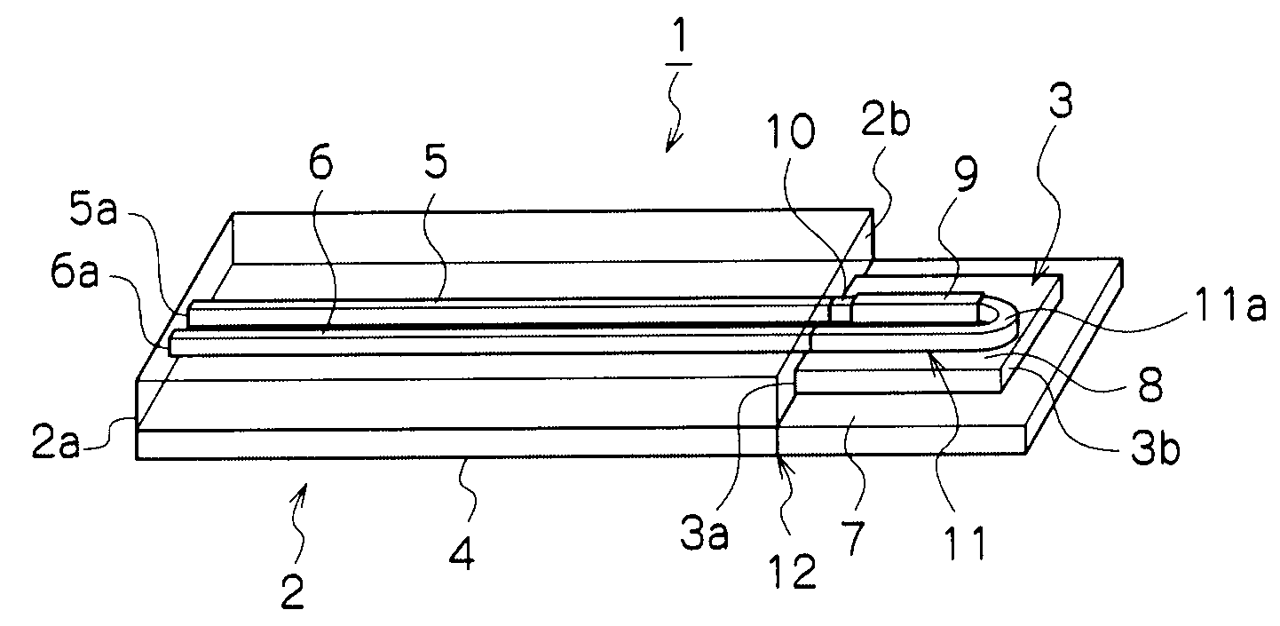
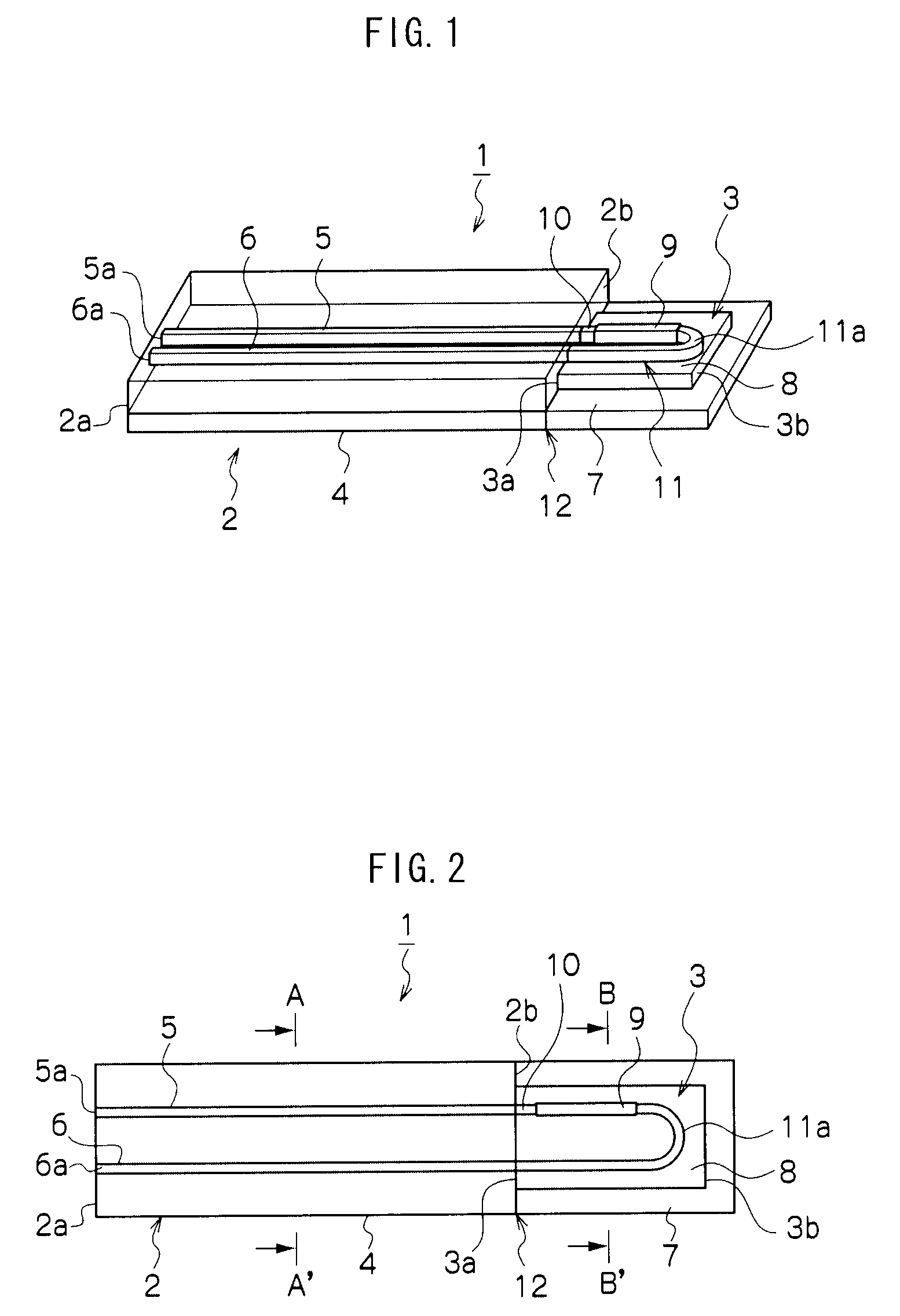
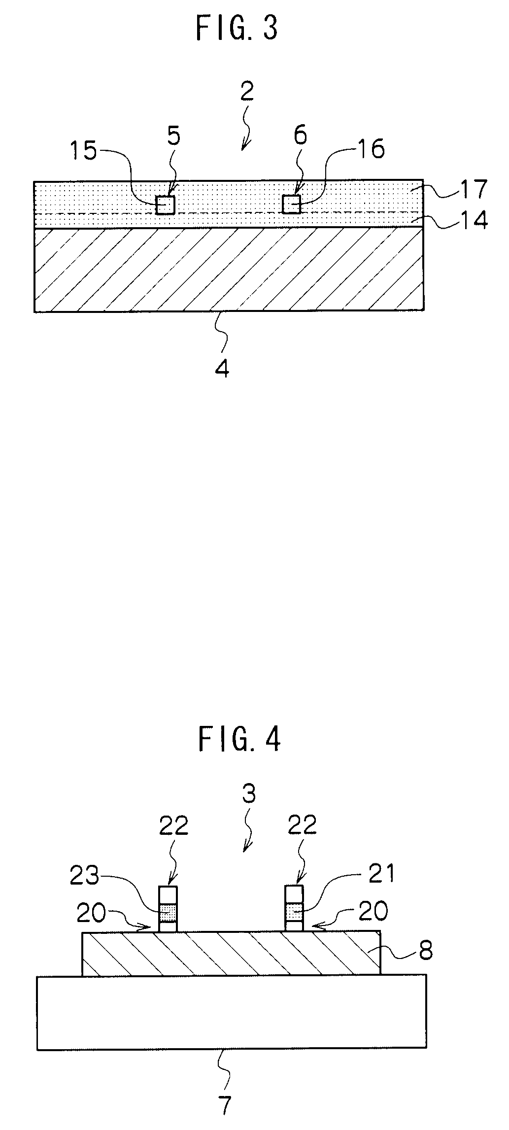
[0045]An optical integrated circuit in accordance with a first embodiment of the present invention will be described based on FIG. 1 through FIG. 4. FIG. 1 is a conceptual diagram showing a basic configuration of the optical integrated circuit in accordance with the first embodiment, while FIG. 2 is a plan view showing the same optical integrated circuit. FIG. 3 is a sectional view along a line A-A′ shown in FIG. 2, and shows a cross-sectional structure of the planar lightwave circuit. Meanwhile, FIG. 4 is a sectional view along a line B-B′ shown in FIG. 2, and shows a cross-sectional structure of a semiconductor waveguide portion of a semiconductor element.

[0046]An optical integrated circuit 1 is a circuit in which a planar lightwave circuit (PLC) 2 and a semiconductor element 3 fixed on a silicon substrate 7 are integrated as shown in FIG. 1 and FIG. 2.

[0047]The planar lightwave circuit 2 is provided with a PLC platform 4 and two straight optical waveguides 5 and 6 formed on the P...

second embodiment

[0071]Next, an optical integrated circuit in accordance with a second embodiment will be described based on FIG. 5 and FIG. 6. FIG. 5 is a conceptual diagram showing a schematic configuration of an optical integrated circuit 1A in accordance with a second embodiment, while FIG. 6 is a plan view showing the optical integrated circuit 1A.

[0072]The optical integrated circuit 1A is characterized in that, in the optical integrated circuit 1 in accordance with the aforementioned first embodiment shown in FIG. 1, a plurality of semiconductor optical amplifiers (elements) are arranged in array pattern on the semiconductor substrate 8 of a semiconductor element 3A. As an example, four semiconductor optical amplifiers 91 to 94 are arranged in array pattern on the semiconductor substrate 8 as shown in FIG. 5 and FIG. 6 in the present embodiment.

[0073]Meanwhile, there are formed on the semiconductor substrate 8 the input semiconductor waveguides 101 to 104 and the output semiconductor waveguide...

third embodiment

[0082]Next, an optical integrated circuit in accordance with a third embodiment will be described based on FIG. 7. FIG. 7 is a conceptual diagram showing a schematic configuration of an optical integrated circuit 1B in accordance with the third embodiment.

[0083]The optical integrated circuit 1B is characterized by following configurations.

[0084]A semiconductor element 3B in which a plurality of waveguide-type photodiodes (elements) 301 to 306 are formed on the semiconductor substrate 8 in array pattern, and a planar lightwave circuit 2B in which a plurality of optical waveguides are formed are fixed at one contact surface 12 and are integrated. As an example, six waveguide photodiodes 301 to 306 are formed on the semiconductor substrate 8 in the present embodiment.

[0085]Six straight optical waveguides 311 to 316 respectively coupled with the light incidence side end facets (light receiving facets) of the waveguide photodiodes 301 to 306 are formed on the PLC platform 4 of the planar...


PUM


Abstract

An optical integrated circuit 1 according to the present invention includes a planar lightwave circuit 2, and a semiconductor element 3, which are fixed at one contact surface 12. A semiconductor optical amplifier (SOA) 9 is formed on a semiconductor substrate 8. A semiconductor waveguide 10 and a semiconductor waveguide 11 are formed on an input side and an output side of SOA 9, respectively. The semiconductor waveguide 11 has a turnaround portion 11a turned around on the semiconductor substrate 8. Respective ends of the optical waveguides 5 and 6 on a PLC platform 4 and respective ends of semiconductor waveguides 10 and 11 are optically coupled with each other at the contact surface 12.

Description

BACKGROUND OF THE INVENTION[0001]1) Field of the Invention[0002]The present invention relates to an optical integrated circuit formed by interconnecting a plurality of optical components, and more specifically, relates to an optical circuit and an optical integrated circuit module. In the optical integrated circuit module, optical hybrid integrated devices, in which a planar lightwave circuit having optical waveguides formed on a PLC platform, and a semiconductor device having optical active components, such as semiconductor laser diodes and semiconductor photodiodes formed on a semiconductor substrate are coupled with each other.[0003]2) Description of the Related Art[0004]With the spread and progress of optical communication networks, functions of optical components for use in optical transmission systems have been sophisticated. The optical components include optical active components for emitting or receiving optical signals, optical passive components for splitting / coupling or ...

Claims


Application Information

Patent Timeline
Patent Type & Authority Patents(United States)
IPC IPC(8): G02B6/12
CPCG02B6/12021G02B6/12004
Inventor FUNABASHI, MASAKIHASEGAWA, JUNICHIAKUTSU, TAKESHINARA, KAZUTAKAYOKOUCHI, NORIYUKI
Owner FURUKAWA ELECTRIC CO LTD
Why Eureka
Try Eureka