

Process for manufacturing semiconductor device
a manufacturing process and semiconductor technology, applied in the direction of solid-state devices, chemical vapor deposition coatings, coatings, etc., can solve the problems of unsuitable mass production techniques for semiconductor devices, low productivity, and the difficulty of forming even films by ald using a single-wafer processing machine, so as to achieve high-quality manufacturing of semiconductor devices. high efficiency
- Summary
- Abstract
- Description
- Claims
- Application Information
AI Technical Summary
Benefits of technology
Problems solved by technology
Method used
Image

Examples
reference example 1
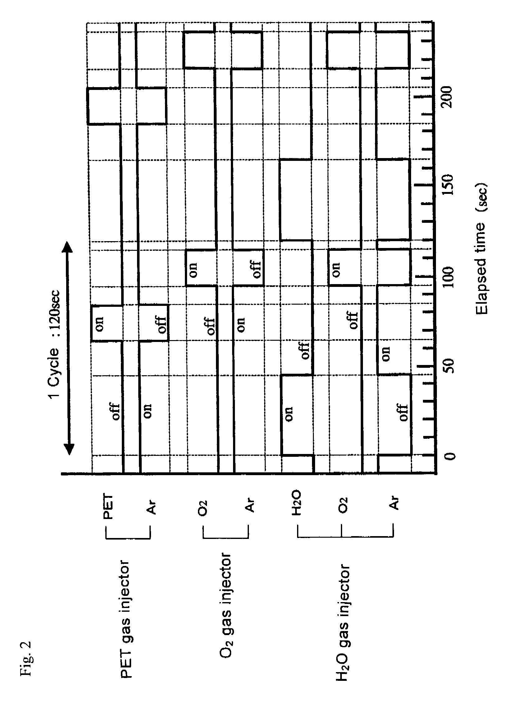
[0120]In Reference Example 1, there will be described a basic gas flow sequence for forming an aluminum oxide film using TMA as a metal source gas and oxidizing O3 as a reactant gas with reference to FIG. 5.
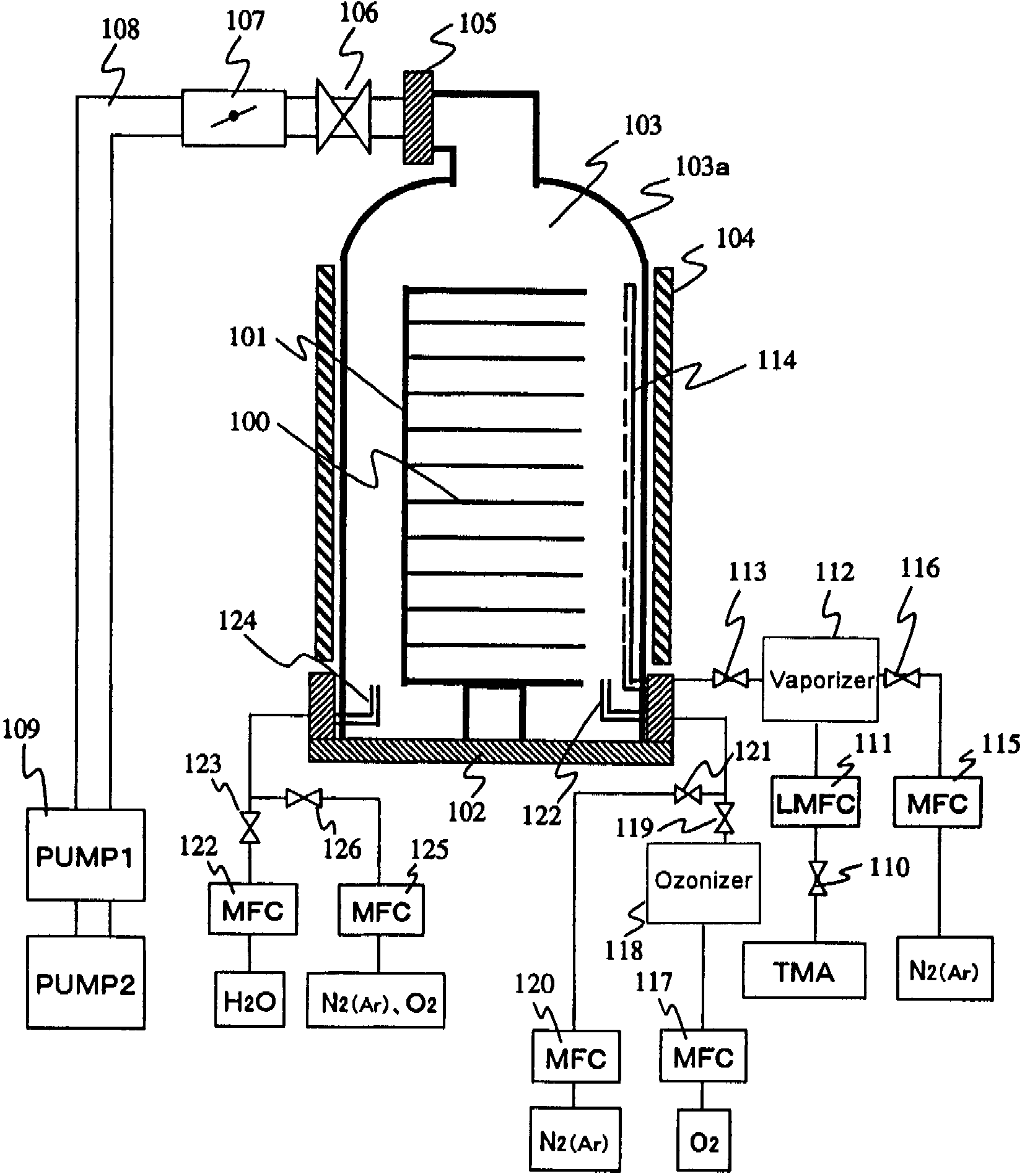
[0121]As shown in FIG. 1, semiconductor substrates 100 (50 sheets) with a diameter of 300 mm were placed in a reaction chamber 103, and N2 was introduced from each gas injector into the reaction chamber and while keeping a pressure at 80 Pa (0.6 Torr), a temperature of the semiconductor substrates 100 was stabilized. After stabilizing the semiconductor substrate 100 at 300° C., an aluminum oxide film was deposited in accordance with the gas flow sequence shown in FIG. 5.
[0122](1) First, on stopping N2 supply from each gas injector, TMA was supplied for 30 sec from a TMA gas injector while keeping a pressure at 80 Pa (FIG. 5, Step 1).
[0123](2) Next, on stopping TMA supply, the pressure-regulating valve 107 shown in FIG. 1 was fully opened and the reaction chamber was vacuum-purged...
example 1
[0129]Example 1 will be described with reference to FIG. 6. Example 1 is different from Reference Example 1 in that the step of supplying O3 is divided into two substeps. Otherwise, Example 1 is as described in Reference Example 1, and its description is not, therefore, repeated.
[0130](1) First, as described in Reference Example 1, on stopping N2 supply from each gas injector, TMA was supplied for 30 sec from a TMA gas injector while keeping a pressure at 80 Pa (FIG. 6, Step 1; the first step).
[0131](2) Next, as described in Reference Example 1, on stopping TMA supply, the reaction chamber was vacuum-purged for 20 sec (FIG. 6, Step 2; the second step).
[0132](3) Then, as described in Reference Example 1, N2 was supplied from each gas injector and the chamber was gas-purged for 20 sec while keeping a pressure at 200 Pa (FIG. 6, Step 3; the third step).
[0133](4) Then, on stopping N2 supply from each gas injector, O3 was supplied for 20 sec from an O3 gas injector while keeping a pressu...
example 2
[0140]Example 2 will be described with reference to FIG. 7. Example 2 is different from Reference Example 1 in that the step of supplying O3 is divided into three substeps. Otherwise, Example 2 is as described in Reference Example 1, and its description is not, therefore, repeated.
[0141](1) First, as described in Reference Example 1, on stopping N2 supply from each gas injector, TMA was supplied for 30 sec from a TMA gas injector while keeping a pressure at 80 Pa (FIG. 7, Step 1; the first step).
[0142](2) Next, as described in Reference Example 1, on stopping TMA supply, the reaction chamber was vacuum-purged for 20 sec (FIG. 7, Step 2; the second step).
[0143](3) Then, as described in Reference Example 1, N2 was supplied from each gas injector and the chamber was gas-purged for 20 sec while keeping a pressure at 200 Pa (FIG. 7, Step 3; the third step).
[0144](4) Then, on stopping N2 supply from each gas injector, O3 was supplied for 10 sec from an O3 gas injector while keeping a pres...
PUM
| Property | Measurement | Unit |
|---|---|---|
| depth | aaaaa | aaaaa |
| diameter | aaaaa | aaaaa |
| size | aaaaa | aaaaa |
Abstract
Description
Claims
Application Information