Semiconductor memory having a precharge voltage generation circuit for reducing power consumption
a technology of pre-charge voltage generation and semiconductor memory, which is applied in the direction of information storage, static storage, digital storage, etc., can solve the problems of electric power consumption and battery dissipation, and achieve the effect of reducing the system cos
- Summary
- Abstract
- Description
- Claims
- Application Information
AI Technical Summary
Benefits of technology
Problems solved by technology
Method used
Image
Examples
first embodiment
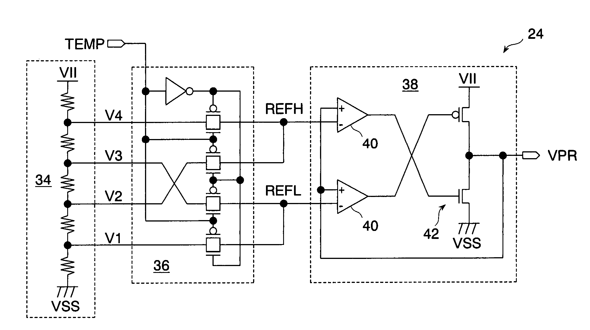
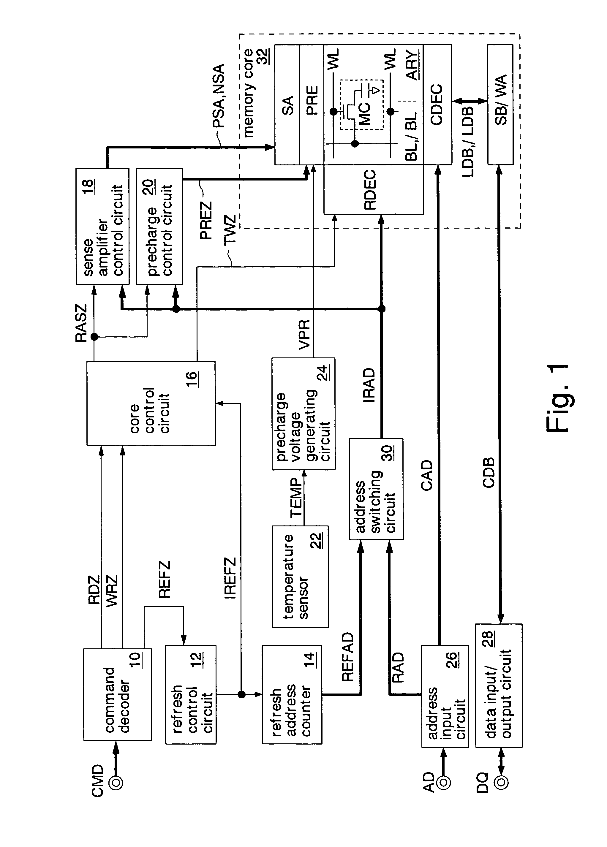
[0036]FIG. 1 shows the semiconductor memory of the invention. This semiconductor memory is formed as a dynamic RAM chip (hereinafter, “DRAM”) by using a CMOS process on a silicon substrate. The DRAM is used as, for example, a work memory which is mounted in a portable equipment such as mobile phone.
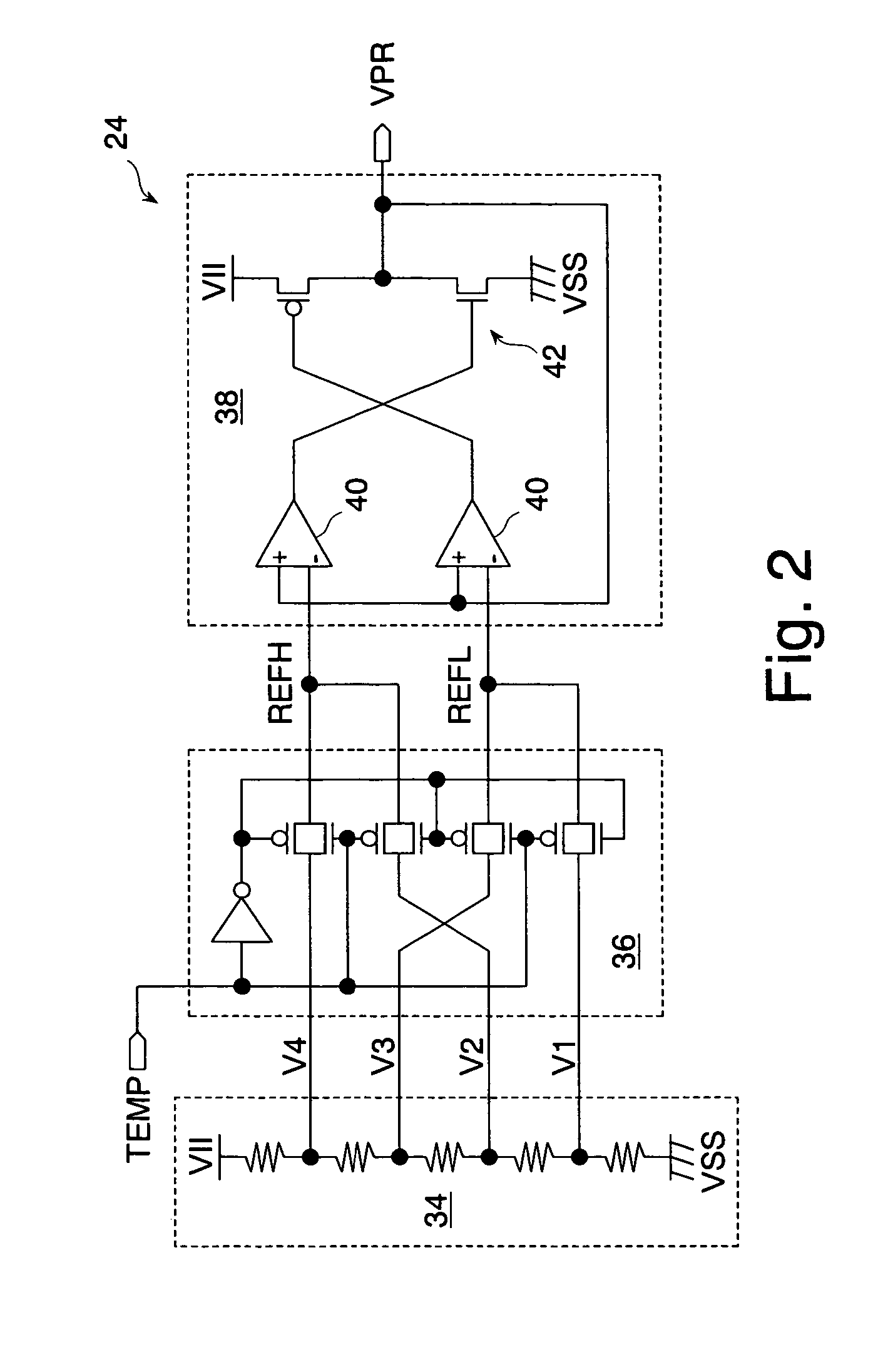
[0037]The DRAM includes a command decoder 10, a refresh control circuit 12, a refresh address counter 14, a core control circuit 16, a sense amplifier control circuit 18, a precharge control circuit 20, a temperature sensor 22, a precharge voltage generating circuit 24, an address input circuit 26, a data input / output circuit 28, an address switching circuit 30 and a memory core 32. Note that, in FIG. 1, only principal signals necessary for the description of the invention are shown.
[0038]The command decoder 10 receives a command signal CMD supplied from an external terminal (for example, a chip select signal / CS, a row address strobe signal / RAS, a column address strobe signal / CAS, and ...
second embodiment
[0081]FIG. 10 shows the relationship between the data retaining time of the DRAM of the second embodiment and the temperature. A thick solid line indicates the data retaining time (worst) of the DRAM of the invention. In this example, the ambient temperature rises to successively shifts into the temperature zones TP1-TP4, and each time the ambient temperature exceeds boundary temperatures BT1, BT2 and BT3, the precharge voltage VPR changes from VPR1 to VPR2, from VPR2 to VPR3, and from VPR3 to VPR4 and lowers gradually. In a case where the ambient temperature falls, reverse changes proceed.
[0082]As thus far described, the same advantages as in the first embodiment can be attained also in the second embodiment. Further, the plurality of kinds of precharge voltages VPR1-VPR4 are switched in accordance with the ambient temperature, whereby the data retaining time can be lengthened more, and the frequency of refreshes can be lowered.
[0083]FIG. 11 shows the third embodiment of the semico...
fourth embodiment
[0091]FIG. 14 shows the operation of the memory core 32 in the case where the “1 data” is read from the memory cell MC, in the The same operations as in FIG. 4 shall be omitted from detailed description. The waveforms of the precharge signal PREZ, word line WL, and sense amplifier activating signals PSA and NSA are the same as in FIG. 4.
[0092]In this embodiment, the precharge voltage VPR is set to be high at the low temperature. The precharge voltage VPR is heightened at the low temperature, whereby the read margin of the “1 data” decreases. At a normal temperature and at a high temperature, the read margin of the “1 data” decreases due to the fall of the cell voltage STR attributed to the junction leak current. Accordingly, the difference between the read margins RM of the “1 data” at the low temperature and at the high temperature becomes small. Incidentally, at the low temperature, a leak current from the memory cell MC is very small, so that the read margin is originally suffic...
PUM
 Abstract
Description
Claims
Application Information


