Zener diode and methods for fabricating and packaging same

a technology of zener diodes and semiconductor layers, applied in the direction of basic electric elements, electrical apparatus, semiconductor devices, etc., can solve the problems of reducing the life of the semiconductor layer, excessive charge flowing into the semiconductor layer to damage or deteriorate the led, and low voltage resistance, so as to reduce the zener impedance value and simplify the process

Inactive Publication Date: 2009-09-01
LG ELECTRONICS INC
View PDF11 Cites 7 Cited by
  • Summary
  • Abstract
  • Description
  • Claims
  • Application Information

AI Technical Summary

Benefits of technology

[0037]The present invention is disclose to solve the afore-mentioned problems, and it is an object of the present invention to provide a zener diode and methods for fabricating and packaging same configured to remove a contact hole forming process exposing the diffusion layers enabling to simplify the process, and reducing a zener impedance value by determining a length of a diffusion layer not contacting an electrode line by a horizontal length of diffused impurity.
[0038]It is another object of the present invention to provide a zener diode and methods for fabricating and packaging same configured to remove a diffusion mask using wet etching following diffusion, enabling to inflict no damage to diffusion layers and thereby improving the zener diode characteristics.
[0039]It is still another object of the present invention to provide a zener diode and methods for fabricating and packaging same configured to use a diffusion layer as an inter-layer insulation film, improving an electrical isolation characteristic between a diffusion layer and a metal line and allowing the diffusion mask and diffusion layer to be self-aligned.

Problems solved by technology

In general, there is a disadvantage in a device having a low voltage-resistance out of semiconductor devices in that its life span is shortened due to static electricity or surge voltage generated during implementation of measurement or packaging process.
Meanwhile, if a reverse surge voltage occurs in a device, for example, a light emitting diode (LED) having a low voltage-resistant characteristic, an excessive charge flows into the semiconductor layer to damage or deteriorate the LED.
These problems can be further worsened if devices are fabricated on top of an insulation substrate.
However, if a contact hole is formed at a region unwanted by the contact hole forming process, a PN zener diode or a resistant body, not a zener diode having a bi-directional threshold voltage characteristic, is formed to lower a yield thereof.
There is another problem in that a current has to flow across a long diffusion layer to increase a zener impedance because the current flows from an electrode line to a diffusion layer and substrate, and flows through another diffusion layer and the other electrode line.
There is still further problem in that a diffusion layer not contacting an electrode line exists due to limitation of contact hole forming process, and the diffusion layer and the electrode line are not self-aligned to result in a deteriorated reliability.
There is still further problem in that if the contact hole is formed by using dry etching, the diffusion layer is damaged by the dry etching to result in a deteriorated characteristic of zener diode.
There is a problem in the process according to the prior art in that, although there is no evaporating process of inter-layer insulation films, the films property-changed at the diffusion mask used for inter-layer insulation films become a cause generating leaked current at the electrode lines, and degrading the characteristics.
There is another problem in that a current flows across the long diffusion layer as described in FIG. 1 of fabricating method to increase the zener impedance value, and if the contact holes are formed using the dry etching, the diffusion layers are damaged by the dry etching to deteriorate the zener diode characteristics.

Method used


Image

  • Zener diode and methods for fabricating and packaging same
  • Zener diode and methods for fabricating and packaging same
  • Zener diode and methods for fabricating and packaging same

Examples


first embodiment

[0058]FIGS. 4a through 4d are cross-sectional views illustrating a fabricating process of a zener diode according to the present invention, where top and bottom insulation films (110.120) are formed on top and bottom of a substrate (100) having a first polarity, and top and bottom mask layers (130.140) are formed on top and bottom insulation layers (110.120) and etching part of the top mask layer (130) and the top insulation film (110) to form a pair of openings (135a. 135b) through which the substrate (100) is exposed. (FIG. 4a)

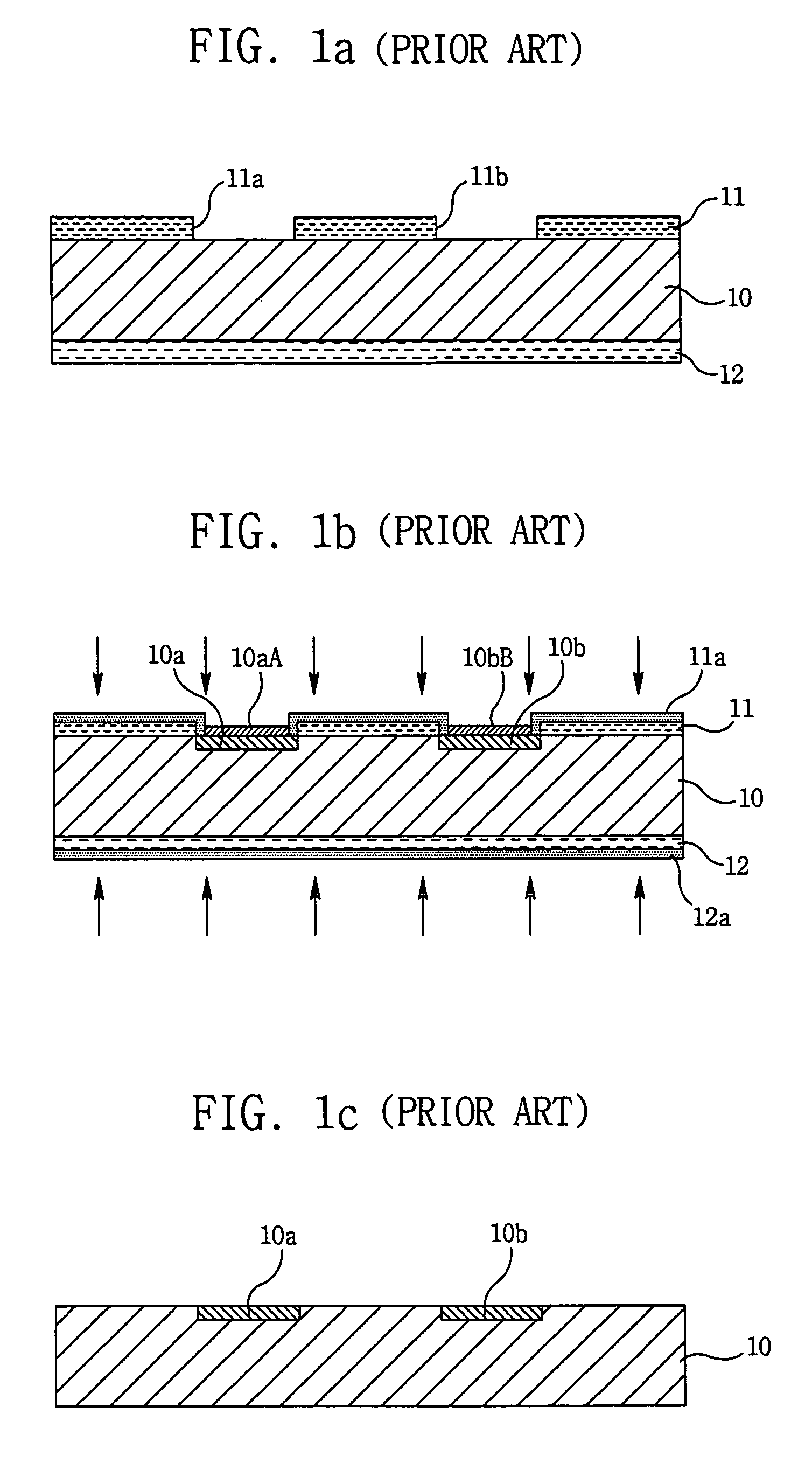
[0059]Preferably, the substrate (100) is silicon substrate.

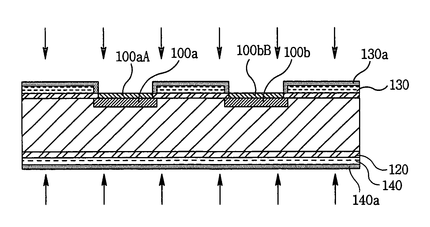
[0060]Next, a diffusion process is conducted by introducing an impurity having a second polarity opposite to that of the first polarity into the top and bottom of the substrate (100) to form diffusion layers (100a.100b) having the second polarity at the substrate (100) region exposed through the pair of openings. (FIG. 4b)

[0061]Through the diffusing process, property-changed films (130a. 130b) are fo...

second embodiment

[0073]FIGS. 6a through 6e are cross-sectional views illustrating a fabricating process of a zener diode according to the present invention.

[0074]First of all, top and bottom insulation films (110.120) are formed on top and bottom of a substrate (100) having a first polarity, and top and bottom insulation films (110.120) are formed thereon and thereunder with top and bottom mask layers (130.140). The top mask layer (130) and the top insulation film (110) are partially etched to form a pair of openings (135a. 135b) through which the substrate (100) is exposed. (FIG. 6a)

[0075]Successively, the substrate (100) is infused thereon and thereunder with impurity having a second polarity opposite to the first polarity, and diffusion process is conducted to form at the substrate (100) region a diffusion layer (100a) having the second polarity. (FIG. 6b)

[0076]Property-changed films (130a. 140a) are formed on the top and bottom mask layers (130.140) through the diffusion process as in the first ...

third embodiment

[0083]FIGS. 7a through 7d are cross-sectional views illustrating a zener diode fabricating process according to the present invention.

[0084]Referring to FIG. 7a, top and bottom mask layers (130.140) are formed on top and bottom of a substrate (100) having a first polarity, and the top mask layer (130) is partially etched to form a pair of openings (135a. 135b) through which the substrate (100) is exposed.

[0085]Successively, the substrate (100) is infused thereon and thereunder with impurity having a second polarity opposite to the first polarity, and diffusion process is conducted to form at the substrate (100) region exposed through the pair of openings (135a. 135b) diffusion layers (100aA, 100bB) having the second polarity. (FIG. 7b)

[0086]Property-changed films (130a. 140a) are formed on the top and bottom mask layers (130.140) through the diffusion process, and diffusion layers (100aA. 100bB) are formed at the surfaces thereof with insulation films.

[0087]Successively, the propert...


PUM


Abstract

A zener diode and methods for fabricating and packaging same are disclosed, whereby contact hole forming process exposing a diffusion layer is removed to enable to simplify the fabricating process, and the diffusion length not contacting the electrode line is determined by the crosswise length toward which the impurity is diffused to enable to reduce the zener impedance value. Furthermore, wet etching is used following the diffusion to remove the diffusion masks such that no damage is given to the diffusion layers to thereby enable to improve the zener diode characteristics.

Description

BACKGROUND OF THE INVENTION[0001]1. Field[0002]This document relates to a zener diode and methods for fabricating and packaging same.[0003]2. Description of the Related Art[0004]In general, there is a disadvantage in a device having a low voltage-resistance out of semiconductor devices in that its life span is shortened due to static electricity or surge voltage generated during implementation of measurement or packaging process. As a protective device against the low voltage-resistance, a zener diode is used.[0005]The zener diode is a diode using a reverse breakdown voltage, and a reverse breakdown of PN zener diode includes a zener breakdown occurring at a low threshold voltage, and an avalanche breakdown occurring at a higher threshold voltage.[0006]The zener breakdown is configured in such a manner that, if an impurity of high concentration is introduced into a semiconductor layer, a charge depletion layer of narrow width is formed to result in generation of a high electric fiel...

Claims


Application Information

Patent Timeline
Patent Type & Authority Patents(United States)
IPC IPC(8): H01L21/20
CPCH01L29/866H01L25/167H01L2224/73265H01L2224/48091H01L2224/48137H01L2924/3011H01L2924/00014H01L2924/00
Inventor SONG, KI CHANGKIM, GEUN HO
Owner LG ELECTRONICS INC
Why Eureka
Try Eureka