Method for forming solder joints for a flip chip assembly

a technology of flip chip and solder joint, which is applied in the manufacture of final products, semiconductor/solid-state device details, printed circuits, etc., can solve the problems and achieve the effect of prolonging the fatigue life of flip chip units

Inactive Publication Date: 2009-10-13
GLOBALFOUNDRIES US INC
View PDF4 Cites 4 Cited by
  • Summary
  • Abstract
  • Description
  • Claims
  • Application Information

AI Technical Summary

Benefits of technology

[0014]There is a need for a method for forming solder joints of a package arrangement that prolongs the fatigue life of flip chip units.

Problems solved by technology

This prolongs the fatigue life of the flip chip units.

Method used


Image

  • Method for forming solder joints for a flip chip assembly
  • Method for forming solder joints for a flip chip assembly
  • Method for forming solder joints for a flip chip assembly

Examples


Embodiment Construction

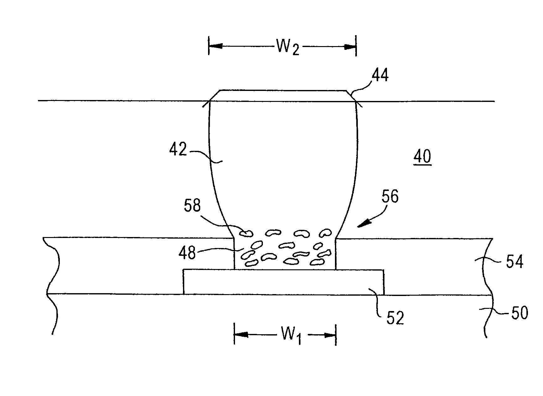
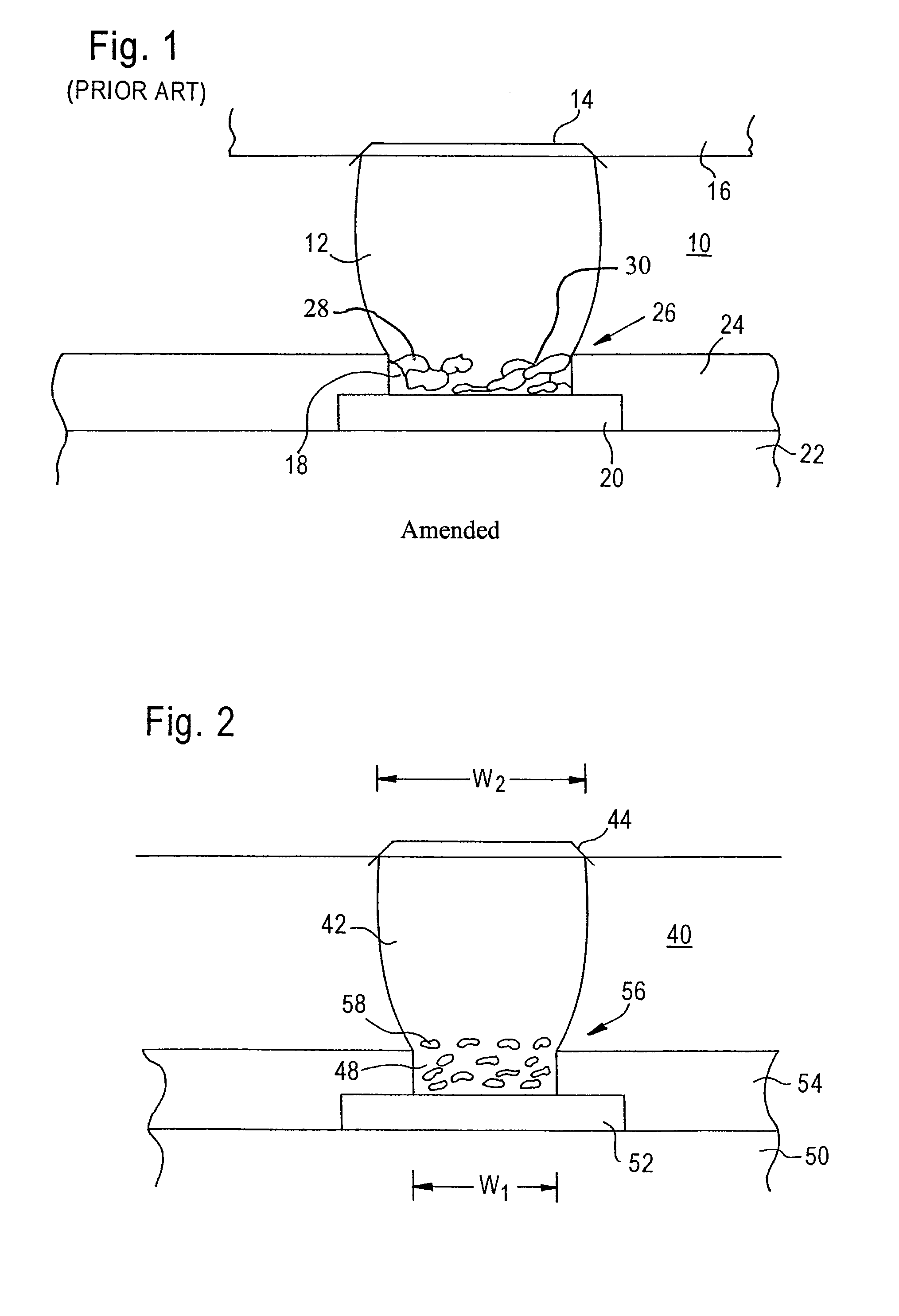
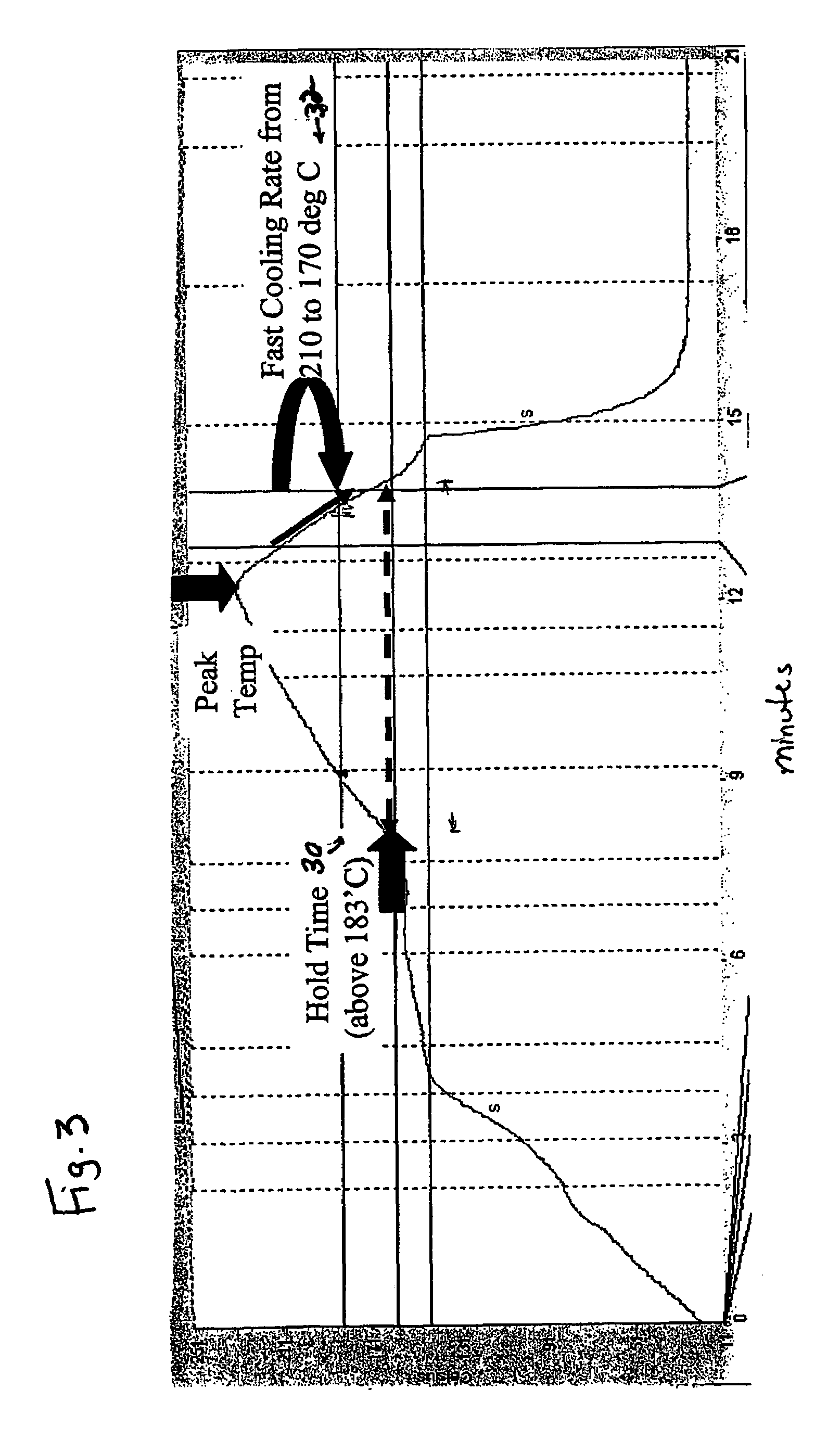
[0025]The present invention addresses and solves problems related to the reliability of eutectic solder joints of flip chips, and seeks to improve the fatigue life of such solder joints. This is achieved, in part, by providing for a eutectic reflow profile that produces more evenly distributed Sn grains, thereby reducing grain boundaries and preventing crack propagation along grain boundaries. In certain embodiments, the eutectic reflow profile includes decreased hold time, higher peak temperature and an increased cooling rate, as compared to prior eutectic reflow profiles. Further, providing a ratio of a width of the pad openings on the solder mask to the width of the under bump metallurgy of approximately 1.0:1.2 to about 1.0:1.6 (and approximately 1.0:1.4 in especially preferred embodiments) also enhances the fatigue life of the arrangement.

[0026]As described, the methodologies for producing eutectic solder joints, and the eutectic reflow profile employed in these methodologies, ...


PUM

PropertyMeasurementUnit
hold timeaaaaaaaaaa
hold timeaaaaaaaaaa
peak temperatureaaaaaaaaaa

Abstract

A method for forming a solder joint for a package arrangement with a dispersed Sn microstructure provides a flip chip on a package, with a flip chip having solder bumps to be connected by eutectic solder joints to pads on the package. The eutectic solder is reflowed at a solder bump/pad interface with a eutectic reflow profile that is configured to achieve eutectic solder joints having substantially evenly distributed Sn grains. The eutectic reflow profile includes an increased cooling rate and decreased hold time with a higher peak temperature. A defined ratio of the pad openings in the solder mask to the under bump metallurgy is provided. The eutectic reflow profile and the defined ratio prolong fatigue life in the package arrangement.

Description

FIELD OF THE INVENTION[0001]The present invention relates to microelectronic packaging of semiconductor chips and, more specifically, to methods for forming package arrangements, such as flip chip assemblies, with prolonged fatigue life for solder joint connections.BACKGROUND OF THE INVENTION[0002]The escalating requirements for high density and performance associated with ultra large scale integration technology creates significant challenges for the design and implementation of electrical connections between circuit components and external electrical circuitry.[0003]Integrated circuit (IC) devices, whether individual active devices, individual passive devices, multiple active devices within a single chip, or multiple passive and active devices within a single chip, require suitable input / output (IO) connections between themselves and other circuit elements or structures. These devices are typically very small and fragile. Because of their size and fragility, they are commonly carr...

Claims


Application Information

Patent Timeline
Patent Type & Authority Patents(United States)
IPC IPC(8): H01L21/00
CPCH01L24/16H05K3/3436H01L24/13H01L2224/131H01L2924/10253H01L2924/01033H01L2224/13016H01L2224/13099H01L2224/16013H01L2924/01082H01L2924/01322H01L2924/14H05K3/3463H05K3/3494H01L2924/01006H01L2924/00H01L2924/014H01L2224/05571H01L2224/05573H01L2924/00014Y02P70/50H01L2224/05599
Inventor MASTER, RAJ N.BAKAR, JUNAIDA A.DING, DIONG H.PARTHASARATHY, SRINIVASAN
Owner GLOBALFOUNDRIES US INC
Why Eureka
Try Eureka