Active matrix type display device, active matrix type organic electroluminescent display device, and methods of driving such display devices

a display device and active matrix technology, applied in static indicating devices, identification means, instruments, etc., can solve the problems of poor conductivity and controllability, difficult problems, and poor crystallization properties of amorphous silicon (non-crystalline silicon) and polysilicon (polycrystalline silicon) to be used for forming tfts, etc., to reduce the area of the pixel circuit occupying, the effect of large area

Inactive Publication Date: 2009-11-03
SONY CORP
View PDF16 Cites 69 Cited by
  • Summary
  • Abstract
  • Description
  • Claims
  • Application Information

AI Technical Summary

Benefits of technology

[0048]In the active matrix type display device having the above configuration or an active matrix type organic EL display device utilizing organic EL elements as the electro-optical elements, the first scanning switch and conversion part are possibly designed to have a large area due to the fact that they deal with a large current as compared with the electro-optical elements. It is noted that the conversion part is used only when luminance information is written, and that the first scanning switch collaborates with the second scanning switch to perform scanning in a row direction (for a selected row). Noting this feature, either or both of the first scanning switch and / or the conversion part may be shared between multiple pixels in a row direction, to thereby decrease the area of the pixel circuit occupying each pixel, which would be otherwise much larger. In addition, if the area of the pixel circuit occupying each pixel is the same, a degree of freedom of layout design increases, so that current can be supplied to the electro-optical element more precisely.

Problems solved by technology

The former displays, however, have some difficult problems when used as a large-size high-precision display, though the display is simple in structure.
However, amorphous silicon (non-crystalline silicon) and polysilicon (polycrystalline silicon) to be used for forming TFTs have poor crystallizing properties as compared with silicon single crystal.
This implies that they have a poor conductivity and controllability, so that TFTs exhibit large fluctuations in characteristics.
However, uniform irradiation of laser light over a large area of the glass substrate is difficult, resulting in non-uniform crystallization of polysilicon at various points on the substrate.
One cannot then anticipate getting a high quality display.
In a case where a current mirror structure as shown in FIG. 3 is employed for the pixel circuit, a problem arises that the structure involves a larger number of transistors as compared with the one as shown in FIG. 1.
This results in a loss of reliability of the pixel caused by increased current density, increased power consumption due to increased drive voltage, coarse graining of the pixels due to the decrease in the light emitting area, and the like, which prevent reduction of the pixel size, namely, hinders an improvement for a higher resolution.
However, there are limitations on the reduction of the channel length L1 in view of withstand voltage of pixels and design rules.
Consequently, dimensional fluctuations in channel length, if they occur on the same panel, can degrade the uniformity of an image formed.
This also causes a large pixel circuit occupying large area.

Method used


Image

  • Active matrix type display device, active matrix type organic electroluminescent display device, and methods of driving such display devices
  • Active matrix type display device, active matrix type organic electroluminescent display device, and methods of driving such display devices
  • Active matrix type display device, active matrix type organic electroluminescent display device, and methods of driving such display devices

Examples


first embodiment

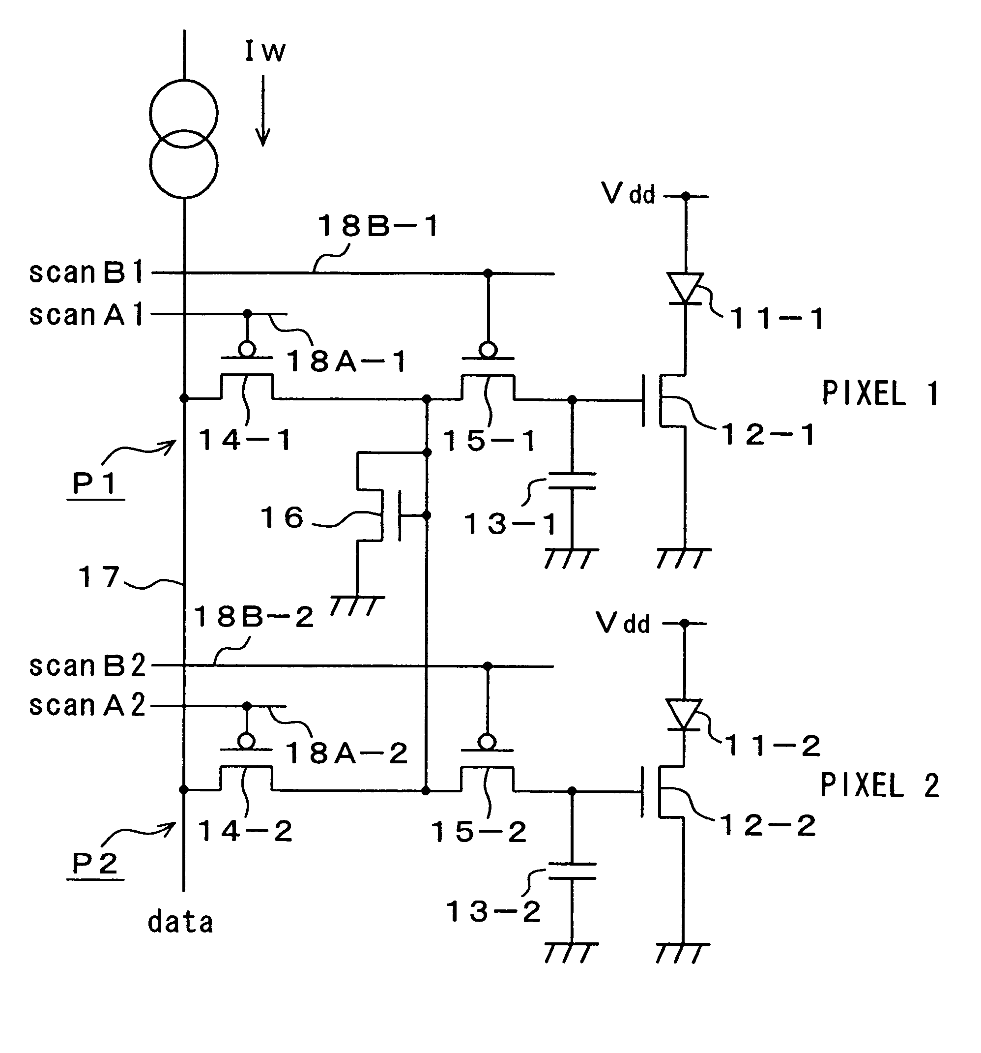
[0075]FIG. 6 illustrates a circuit diagram of a first embodiment of a current-writing type pixel circuit according to the invention, in which only two neighboring pixels (pixel 1 and 2) in a column are shown for simplicity's sake in drawing.

[0076]As shown in FIG. 6, the pixel circuit P1 of pixel 1 comprises OLED (organic EL element) 11-1 having an anode connected to a positive voltage supply Vdd, a TFT 12-1 having a drain connected to a cathode of the OLED 11-1 and a grounded source, a capacitor 13-1 connected to a gate of the TFT12-1 and the ground (reference potential point), a TFT 14-1 having a drain connected to a data line 17 and a gate connected to a first scanning line 18A-1, respectively, a TFT 15-1 having a drain connected to a source of TFT 14-1, a source connected to the gate of the TFT 12-1, and a gate connected to a second scanning line 18B-1, respectively.

[0077]Similarly, the pixel circuit P2 of pixel 2 comprises OLED 11-2 having an anode connected to the positive volt...

second embodiment

[0115]FIG. 13 is a circuit diagram showing a second embodiment of a current-writing type pixel circuit according to the invention. Like reference numerals in FIGS. 13 and 6 represent like or corresponding elements. Here, for simplicity of illustration, only two neighboring pixels (pixels 1 and 2) in a column are shown.

[0116]As compared to the first embodiment in which a current-voltage conversion TFT 16 is shared between two pixels, the pixel circuit of the second embodiment has an the first scanning TFT 14 serving as a first scanning switch is also shared between two pixels. That is, regarding “A” group of scanning lines, one scanning line 18A is provided to every two pixels, and the gate of single scanning TFT 14 is connected to the scanning line 18A, and the source of the scanning TFT 14 is connected to the drain and the gate of the current-voltage conversion TFT 16 and to the drains of the scanning TFTs 15-1 and 15-2 serving as a second scanning switch.

[0117]The scanning line 18...


PUM


Abstract

When a current-writing type pixel circuit is made, it involves a greater number of transistors and TFTs occupy much of the area of the pixel circuit. To alleviate this problem, two pixel circuits (P1, P2) have a first scanning TFT (14), a current-voltage conversion TFT (16), respective second scanning TFTs (15-1, 15-2), capacitors (13-1, 13-2), and drive TFTs (12-1, 12-2) for OLED including organic EL elements (11-2, 11-2) of two pixels, for example, in a row direction. In each of the pixel circuits, the first scanning TFT (14) handling a large amount of current (Iw) as compare with current flowing through the OLED (11-2, 11-2), and the current-voltage conversion TFT (16) are shared between two pixels.

Description

RELATED APPLICATION DATA[0001]The present application is a divisional of U.S. application Ser. No. 10 / 221,402, filed Sep. 11, 2002, now U.S. Pat. No. 7,019,717, which is a U.S. National Phase Application of PCT / JP02 / 00152, filed Jan. 11, 2002, which claims priority to Japanese Patent Application No. P2001-006387, filed Jan. 15, 2001, all applications are incorporated herein by reference to the extent permitted by law.TECHNICAL FIELD[0002]The invention relates to an active matrix type display device having an active element provided in each pixel wherein the active element performs a display control in pixel units, and to a method of driving the same. More particularly, it relates to an active matrix type display device having electro-optical elements whose luminance varies with the current flowing therethrough, as display elements for the pixel and to an active matrix type organic electroluminescent display device which utilizes organic electroluminescent (hereinafter called organic...

Claims


Application Information

Patent Timeline
Patent Type & Authority Patents(United States)
IPC IPC(8): G09G3/30G09F9/30G09G3/20H01L51/50G09G3/32H01L27/32H05B44/00
CPCG09G3/30G09G3/3241G09G3/3266G09G2310/0262G09G2300/0804G09G2300/0842G09G2300/0465
Inventor YUMOTO, AKIRAASANO, MITSURU
Owner SONY CORP
Why Eureka
Try Eureka