

Phase change material for high density non-volatile memory
a non-volatile memory and phase change technology, applied in the field of phase change materials for high-density non-volatile memory, can solve the problems of 50% of electric power and no substantial improvement, and achieve the effect of reducing power consumption and thermal interference between memory cells
- Summary
- Abstract
- Description
- Claims
- Application Information
AI Technical Summary
Benefits of technology
Problems solved by technology
Method used
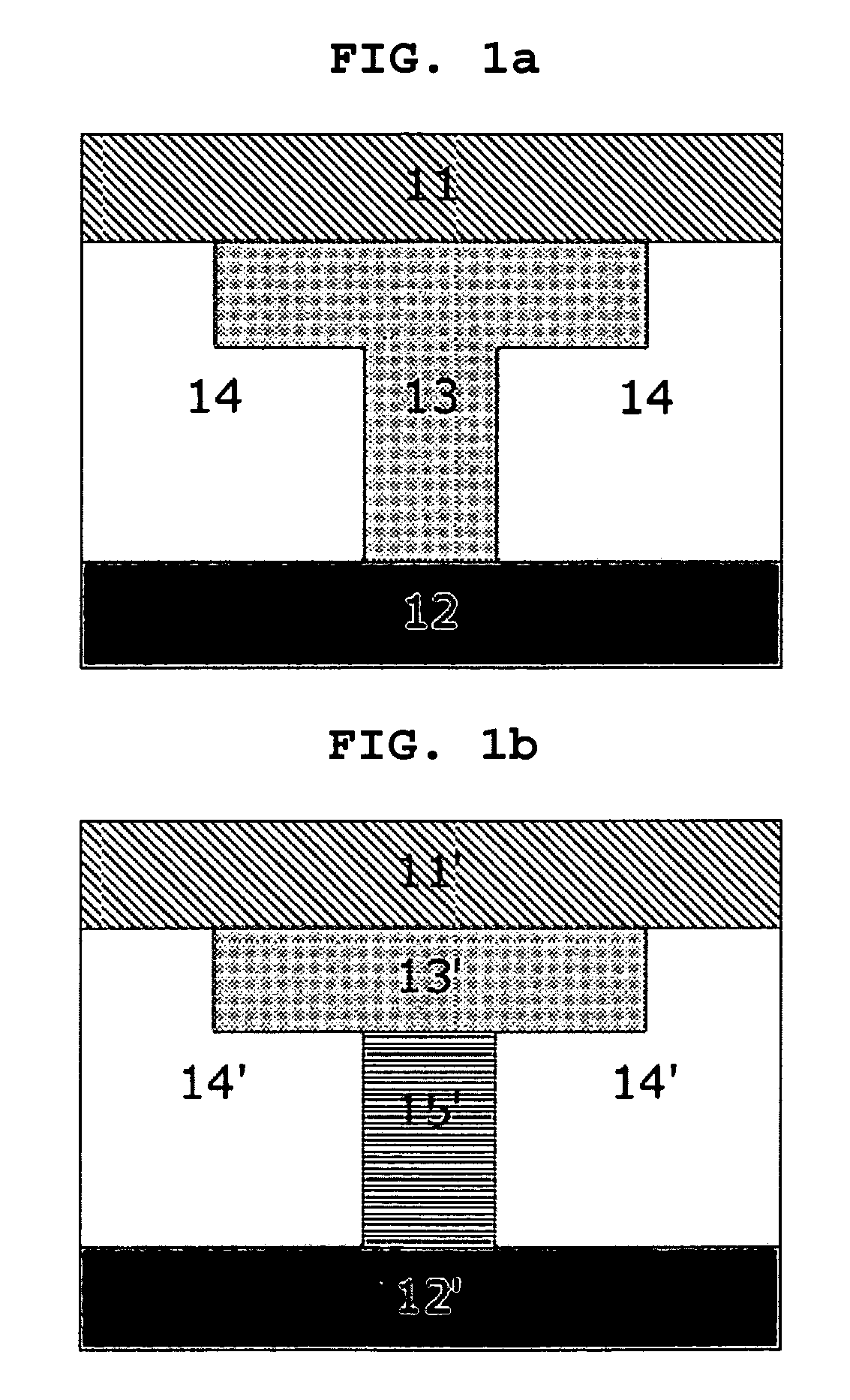
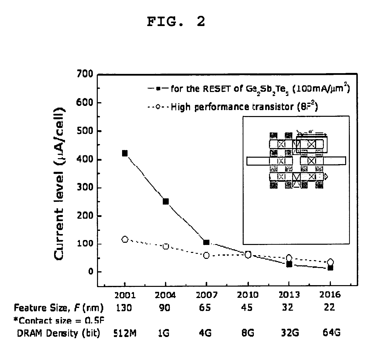
Image

Examples
example
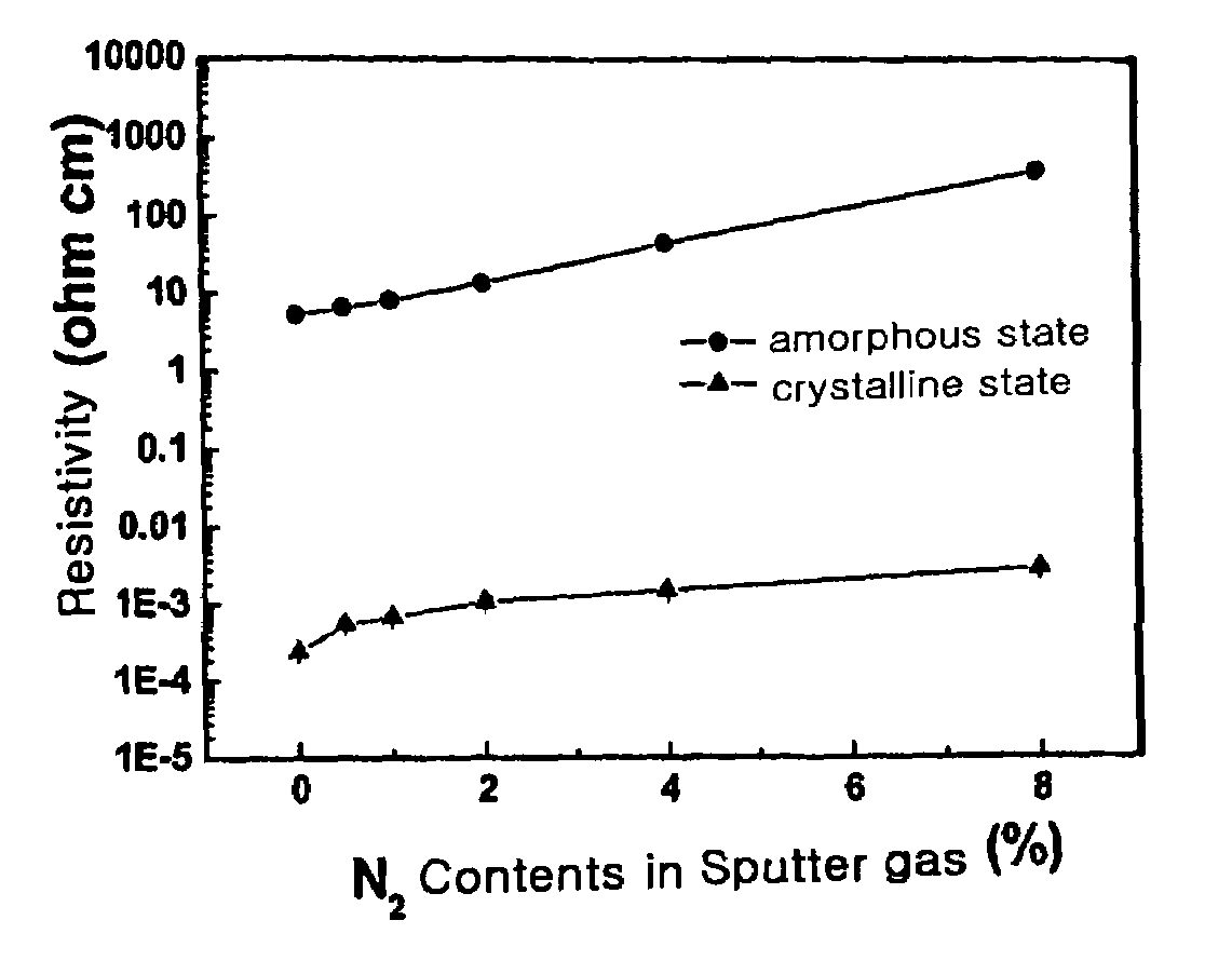
[0058]Ge—Sb—Te—N films were fabricated by a reactive RF magnetron sputter method employing Ge5Sb75Te20 (Mitsubishi Materials Co.) as a sputter target. A mixture of Ar and nitrogen was employed as the sputter gas at 2 mTorr and at a fixed power of 25 W. For thermal analysis, a stainless steel foil was employed as a substrate. A 2 μm-thick film was formed on the stainless steel foil, which was then crumpled to collect film debris. For the purpose of measuring the electrical resistivity, 100 nm-thick films were also fabricated on glass substrates.
[0059]FIG. 5a is a graph showing differential scanning calorimetry (DSC) data for three samples obtained using sputter gases of varying N2 content (expressed in terms of percentile ratio of N2 gas flow rate with respect to the total gas flow rate), and FIG. 5b, the influence of the N2 content in the sputter gas on the crystallization temperature and the melting temperature. The scanning rates were 5° C. / min (FIG. 5a) and 10° C. / min (FIG. 5b), ...
PUM
| Property | Measurement | Unit |
|---|---|---|
| melting temperature | aaaaa | aaaaa |
| melting temperature | aaaaa | aaaaa |
| melting temperature | aaaaa | aaaaa |
Abstract
Description
Claims
Application Information