Semiconductor unit having two device terminals for every one input/output signal

Inactive Publication Date: 2009-12-15
KOMORO MURATA MFG +1
View PDF14 Cites 60 Cited by
  • Summary
  • Abstract
  • Description
  • Claims
  • Application Information

AI Technical Summary

Benefits of technology

[0008]It is therefore an object of the present invention to provide a semiconductor unit, a semiconductor module, and a memory

Problems solved by technology

However, when the memory system further operates at the high-speed, problem arise in distortion of the signal waveform generated because the signal reflected at an end portion of an intra-package wire goes and returns the intra-package wire in the manner which will later become clear.
In addition, in the memory system where the intra-package wire branches the signal path, there is a limit in a high-speed of the operating frequency.
However, in JP-A 2001-68617, inasmuch as the signal wires extending in parallel with the substrate pass through directly below the semiconductor elements for a long section, problems arise where cross-talk noises (electromagnetic coupling noises) are superimposed from the signal wiring to signal wires within the semiconductor elements and power-supply wires when the operating frequency becomes the high-speed.
In addition, problems arise where when laminating of the semiconductor elements are carried out, heat generated from the semiconductor elements concentrates, temperature of the module increases, and degradation of performance is caused.
Specifically, in the command address wires, it is necessary to distribute signals from resisters mounted on the memory module to all of the memory devic

Method used


Image

  • Semiconductor unit having two device terminals for every one input/output signal
  • Semiconductor unit having two device terminals for every one input/output signal
  • Semiconductor unit having two device terminals for every one input/output signal

Examples


second embodiment

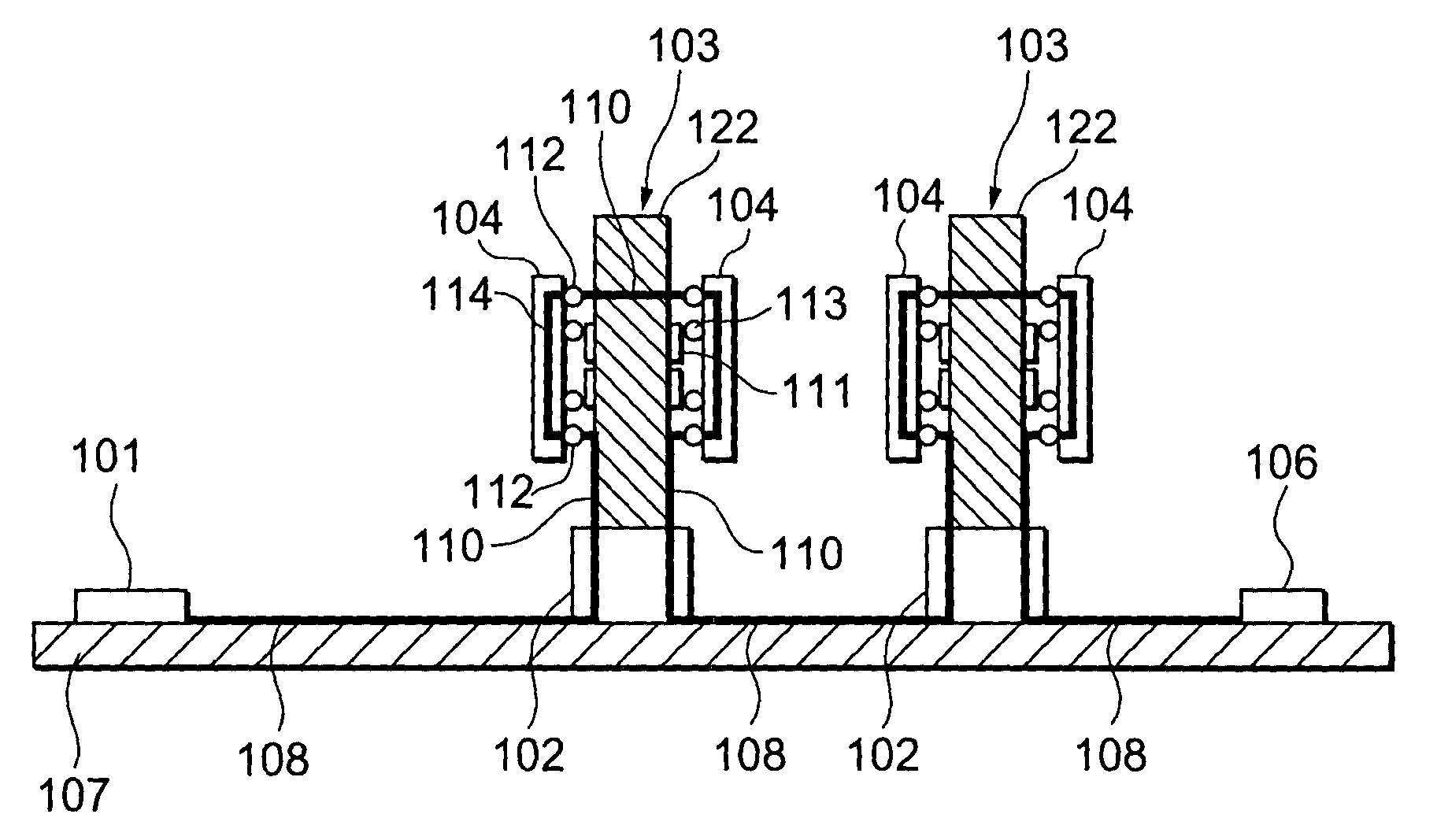
[0116]FIG. 8 shows details of the memory device 104 for use in a memory system according to this invention. The memory device 104 of this embodiment comprises the memory chip 120 and the package substrate 121 having a size larger than that of the memory chip 120. The package substrate 121 has structure where contacts enable to pick out from a surface opposite to the device terminals such as the DQ pins 112, the power supply pins 116, 117. If the memory devices 104 illustrated in FIG. 8 are piled up to two-stage, a second stage of device terminals are connected to the contacts formed on a first stage of the memory device 104, and it is possible to easily obtain a layered structure.

[0117]FIG. 9 shows structure of the memory system according to the second embodiment of this invention. The memory system 100 according to the second embodiment is different from that according to the first embodiment in a point where the memory system comprises dual-system of data bus terminated in one mem...

third embodiment

[0133]In this invention, the signal input terminal pad 115A for inputting the signal for the memory chip 120 and the signal output terminal pad 115B for outputting the signal are comprised as different pads. In this event, it is possible for the package substrate 121 to constitute a line of wires with no branch from one DQ pin 112 to another DP pin 112 of the memory device 104 and a signal transmission characteristic is further improved.

[0134]Although the memory device 104 adopts a structure where the package substrate 121 having wiring layers is put on the memory chip 120 in the above-mentioned embodiment, it may use a tape material having a layered structure in place of the package substrate 121. Although impedance of each wire in the package substrate 121 may be adjusted a thickness of the wire, a width of the wire, an interval between wires, material of the wiring layer or an insulating layer, a structure of the wire, or the like, it may be adjusted by adding a capacitance eleme...


PUM


Abstract

A semiconductor unit constituting a memory device has a memory chip, a package substrate having three wiring layers. Power-supply surfaces (VDD surface) and (GND surface) are wired on the package substrate while an intra-package DQ bus is wired on an intermediate layer between both of the power-supply surfaces. The memory device has two DQ pins every one intra-package DQ bus. The intra-package DQ bus is connected to a signal terminal pad of the memory chip through a via hole. In view of the two DW pins, a via hole for connecting the intra-package DQ bus with the signal terminal pad constitutes a branch wire.

Description

BACKGROUND OF THE INVENTION[0001]This invention relates to a semiconductor unit, a semiconductor module, and a memory system and, in particular, to a semiconductor unit, a semiconductor module, and a memory system where degradation of data signals or the like hardly occurs on high-speed operation.[0002]Recent years, demand for high-speed becomes high more and more in a memory system. Specifically, in a high-speed memory system, performance coping with a high frequency such as hundreds of MHz through several GHz is required. In general, in the memory system, when a operation frequency becomes high, a waveform is easily confused on propagating of a signal on a wire. Accordingly, device is performed to a signal wiring so that a signal propagates accurately and a high-speed.[0003]For example, United State Patent Application Publication No. US 2001 / 0024389 A1 discloses a memory system operable at a high-speed in which branches of the signal wiring are cut and reflection of a signal occur...

Claims


Application Information

Patent Timeline
IPC IPC(8): H01L23/538G06F12/00G06F13/16G11C5/00G11C11/24H01L23/12H01L23/52H01L25/065H01L25/07H01L25/18
CPCH01L23/552H01L23/60H01L23/64H01L24/06H01L25/105H05K1/14H05K1/181H01L23/50H01L2924/13091H01L2224/05554H01L2224/05553H01L2225/107H01L2225/1058H01L2225/1023H01L24/49H01L2924/01033H01L2924/01005H01L2924/00014H01L24/48H05K2201/10545H01L2223/6627H01L2224/04042H01L2224/05599H01L2224/06136H01L2224/48091H01L2224/4824H01L2224/49171H01L2224/85399H01L2924/01004H01L2924/01006H01L2924/0102H01L2924/01029H01L2924/014H01L2924/15173H01L2924/15192H01L2924/15311H01L2924/1532H01L2924/15331H01L2924/19032H01L2924/19041H01L2924/19051H01L2924/19106H01L2924/30107H01L2924/3011H01L2924/3025H05K1/112H05K2201/09236H05K2201/10159H01L2224/45099H01L2924/00H01L2924/30111Y02P70/50
Inventor FUNABA, SEIJIABO, HISASHIONO, TAKAOHOSOKAWA, KOJINISHIO, YOJINAKAMURA, ATSUSHISATO, TOMOHIKO
Owner KOMORO MURATA MFG
Why Eureka
Try Eureka