

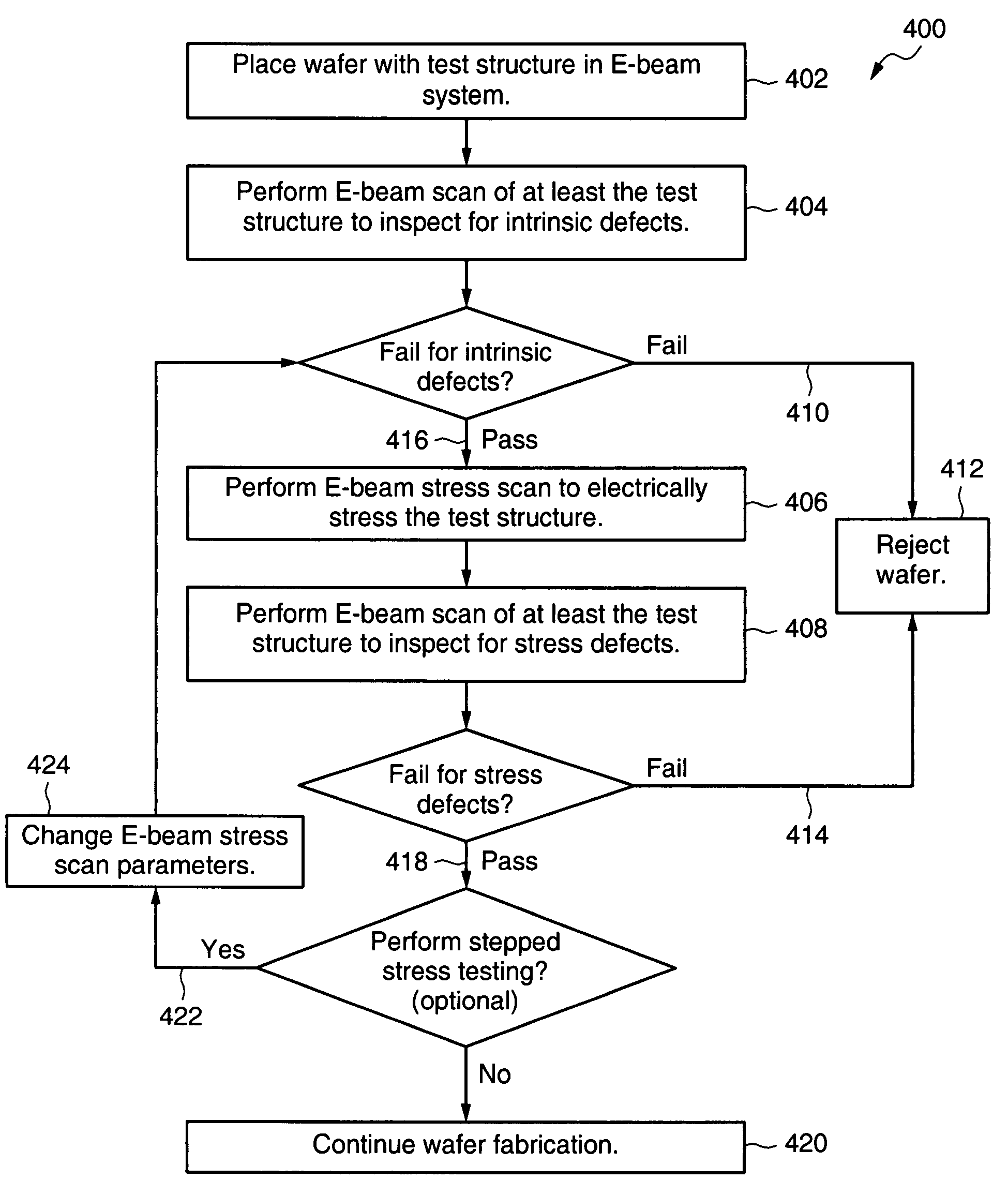
In-line reliability test using E-beam scan
a technology of e-beam scan and reliability test, which is applied in the direction of material analysis using wave/particle radiation, semiconductor/solid-state device testing/measurement, instruments, etc., can solve the problems of destroying the operability of the fet, and affecting the reliability of the tes
- Summary
- Abstract
- Description
- Claims
- Application Information
AI Technical Summary
Benefits of technology
Problems solved by technology
Method used
Image

Examples
Embodiment Construction
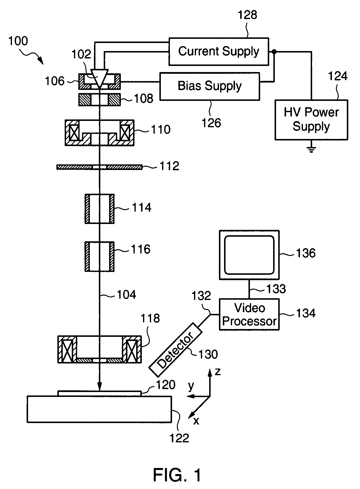
[0025]FIG. 1 is a diagram of an exemplary E-beam system 100. E-beam systems are well known in the art of IC inspection; therefore, a detailed description of the components and operation of an E-beam are omitted. Those of skill in the art appreciate that FIG. 1 and its associated description are simplified. The E-beam system has an electron gun with a cathode 102 that produces an electron beam 104. The electron beam passes through an emission control electrode 106, an anode 108, a condenser lens 110, an aperture 112, deflectors 114, 116 and an objective lens 118 to a sample 120, such as an IC wafer or an IC chip. The sample 120 is supported by a stage 122. The stage 122 is typically movable in at least the X and Y directions.
[0026]A high-voltage (“HV”) power supply 124 is typically kept at a constant voltage (e.g., 10-20 KeV) and a bias supply 126 connected to the emission control electrode 106 controls the energy of electrons emitted by the cathode 102 at the sample 120. A current s...
PUM
| Property | Measurement | Unit |
|---|---|---|
| temperature | aaaaa | aaaaa |
| test structure | aaaaa | aaaaa |
| electrically stress | aaaaa | aaaaa |
Abstract
Description
Claims
Application Information