

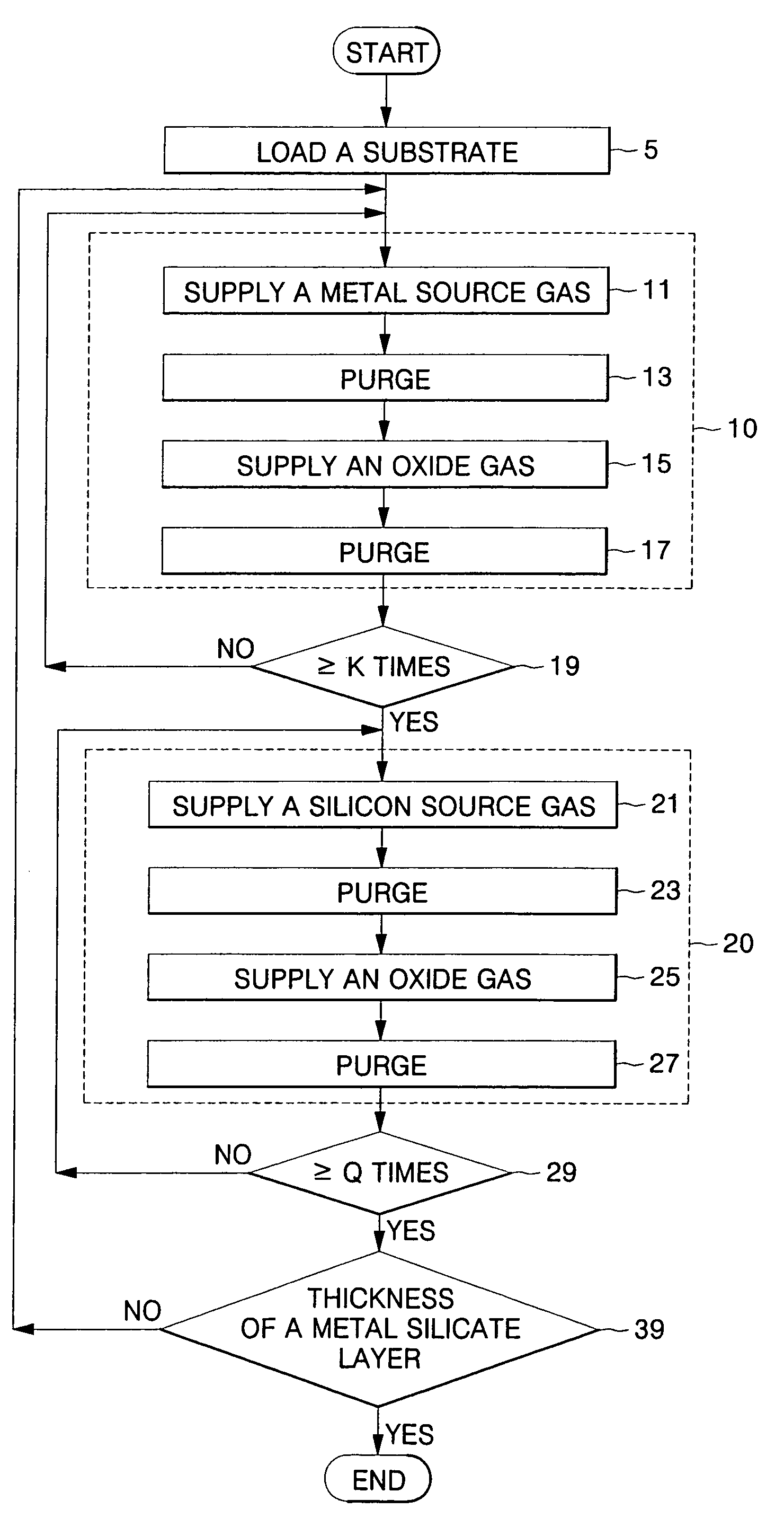
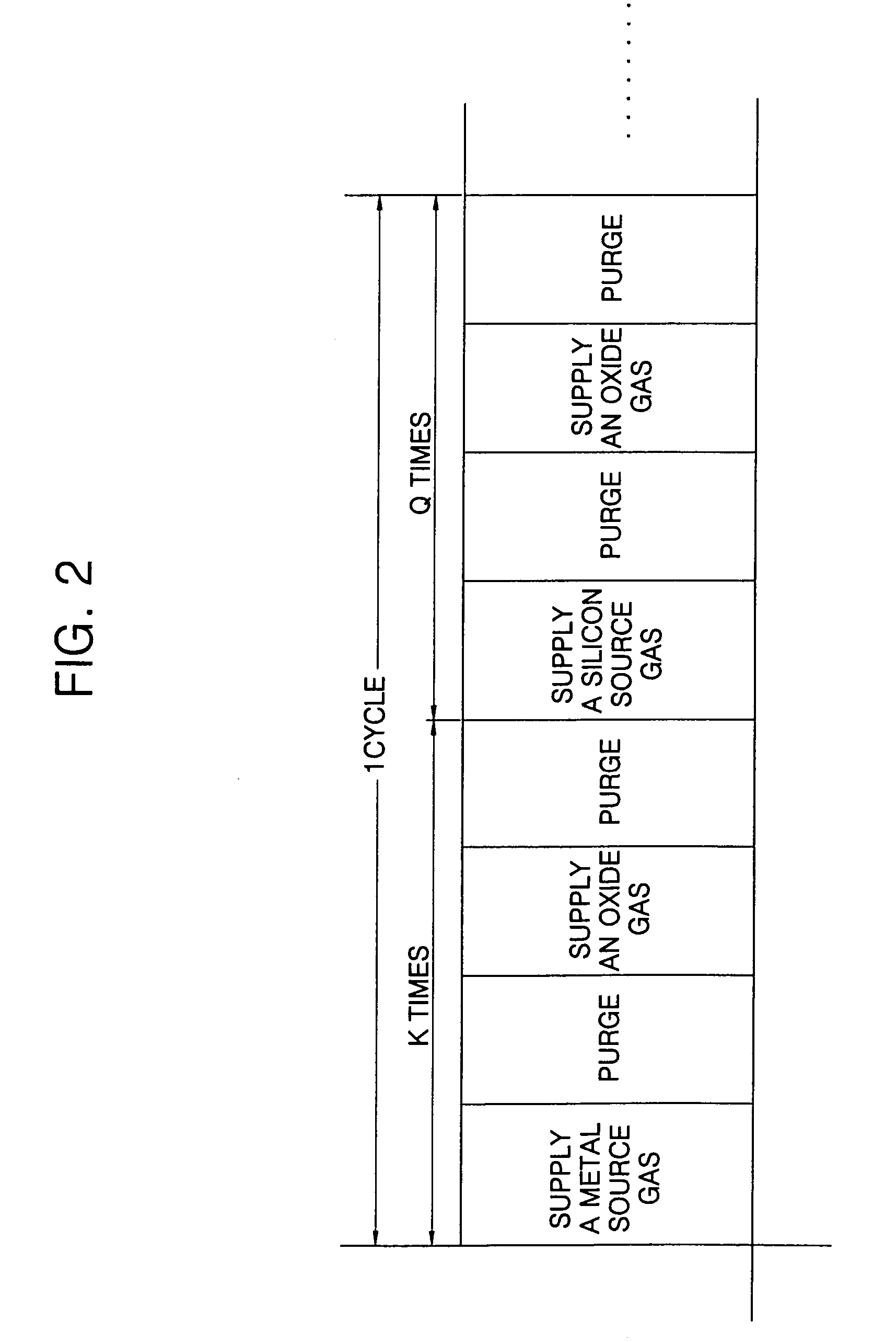
Method of fabricating metal silicate layer using atomic layer deposition technique
a metal silicate and atomic layer technology, applied in the direction of metal material coating process, digital storage, instruments, etc., can solve the problems of deterioration of the insulation characteristics of the gate dielectric layer, rapid increase of leakage current, and many difficulties in fabrication
- Summary
- Abstract
- Description
- Claims
- Application Information
AI Technical Summary
Benefits of technology
Problems solved by technology
Method used
Image

Examples
experiment examples
[0067]FIG. 3 is a graph illustrating thicknesses of different hafnium silicate layers formed on a semiconductor substrate according to embodiments of the present invention. A horizontal axis P in the graph of FIG. 3 represents measured positions of the semiconductor substrate, and the measured positions are spaced by 7 mm downward from the center of the semiconductor substrate. A vertical axis T in the graph of FIG. 3 represents measured thickness, and the unit of thickness is Å. In the three experiment examples shown in FIG. 3, the same temperature of the reactor, deposition pressure, and pulse time of supplying the hafnium source gas, among the various process conditions for forming the hafnium silicate layer, were used for comparison. In specific, the temperature of the reactor was set at 320° C., and the deposition pressure was set at 0.2 torr. Further, the pulse time of supplying the hafnium source gas was 0.2 seconds.
[0068]Referring to FIG. 3, a curve A shows the result of the...
PUM
| Property | Measurement | Unit |
|---|---|---|
| temperature | aaaaa | aaaaa |
| time | aaaaa | aaaaa |
| pulse time | aaaaa | aaaaa |
Abstract
Description
Claims
Application Information