MEMS resonator and manufacturing method of the same

a technology of resonators and manufacturing methods, applied in semiconductor devices, semiconductor/solid-state device testing/measurement, nanotechnology, etc., can solve the problems of increased noise, increased cost, increased noise, etc., and achieves the effect of simplifying processes, reducing costs, and simplifying processes

Inactive Publication Date: 2010-03-02
SEIKO EPSON CORP
View PDF15 Cites 13 Cited by
  • Summary
  • Abstract
  • Description
  • Claims
  • Application Information

AI Technical Summary

Benefits of technology

[0006]An advantage of the invention is to provide a method for manufacturing a MEMS resonator which simplifies processes and reduces the costs, as well as to provide a MEMS resonator produced with the method.
[0007]According to a first aspect of the invention, a method for manufacturing a MEMS resonator includes the following steps. Forming a lower electrode of an ONO capacitor unit included in the semiconductor device using a first silicon layer; forming, using a second silicon layer, a substructure of the MEMS structure unit and an upper electrode of the ONO capacitor unit included in the semiconductor device; and forming, using a third silicon layer, a superstructure of the MEMS structure unit and a gate electrode of a CMOS circuit unit included in the semiconductor device. Here, the MEMS resonator includes a semiconductor device and a MEMS structure unit that are formed on a substrate.
[0008]With the above method, the MEMS structure, the CMOS circuit, and the ONO capacitor are packaged on a single chip. This not only simplifies the process and reduces the cost but also simplifies the system and makes the system effective against noise.
[0009]According to a second aspect of the invention, a MEMS resonator includes a MEMS structure unit formed on the substrate, and a semiconductor device formed on a substrate, the semiconductor device including an ONO capacitor unit and a CMOS circuit unit.
[0010]With the above method, the MEMS structure, the CMOS circuit, and the ONO capacitor are packaged on a single chip. This not only simplifies the process and reduces the cost, but also simplifies the system and makes the system effective against noise.
[0011]In this case, the MEMS resonator may include: a first silicon layer used for forming a lower electrode included in the ONO capacitor unit; a second silicon layer used for forming a substructure included in the MEMS structure unit and an upper electrode included the ONO capacitor unit; and a third silicon layer used for forming a superstructure included in the MEMS structure unit and a gate electrode included in the CMOS circuit unit.

Problems solved by technology

The above resulted in the following problems.
If the ONO capacitor is not included and therefore not used, limitations are imposed on the structure (less variations) of the CMOS circuits such as analog-digital conversion circuit, and other circuits requiring capacitor other than substrate electrode.
Moreover, a system in package (SIP) structure in which the ONO capacitor is packaged in a separate chip results in problems such as increased number of processes, increased cost, and noises generated by a wire bonding of interconnections.
If the MEMS structure is not included, it results in the aforementioned problems such as increased noise.
This causes an increase in the number of processes and costs, since the processing steps cannot be carried out concurrently.

Method used


Image

  • MEMS resonator and manufacturing method of the same
  • MEMS resonator and manufacturing method of the same
  • MEMS resonator and manufacturing method of the same

Examples


Embodiment Construction

[0018]Embodiments in which the invention is applied will now be described with references to the accompanying drawings.

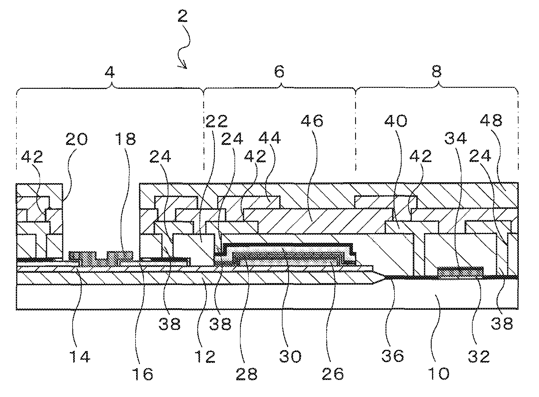
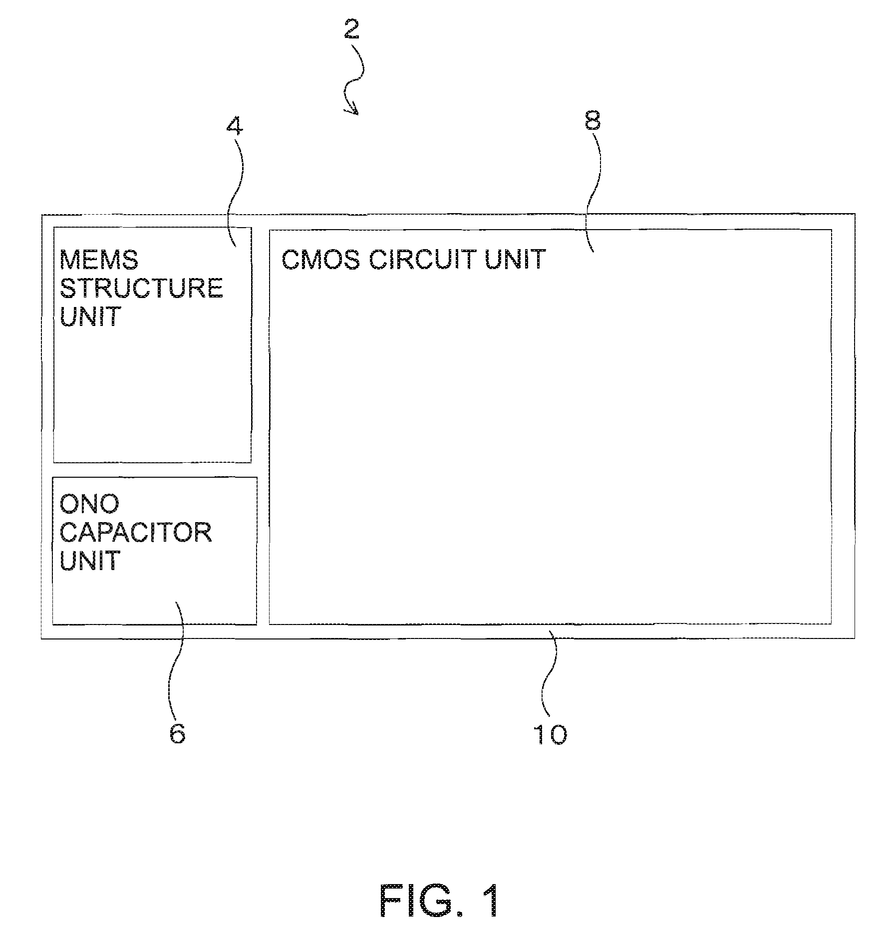
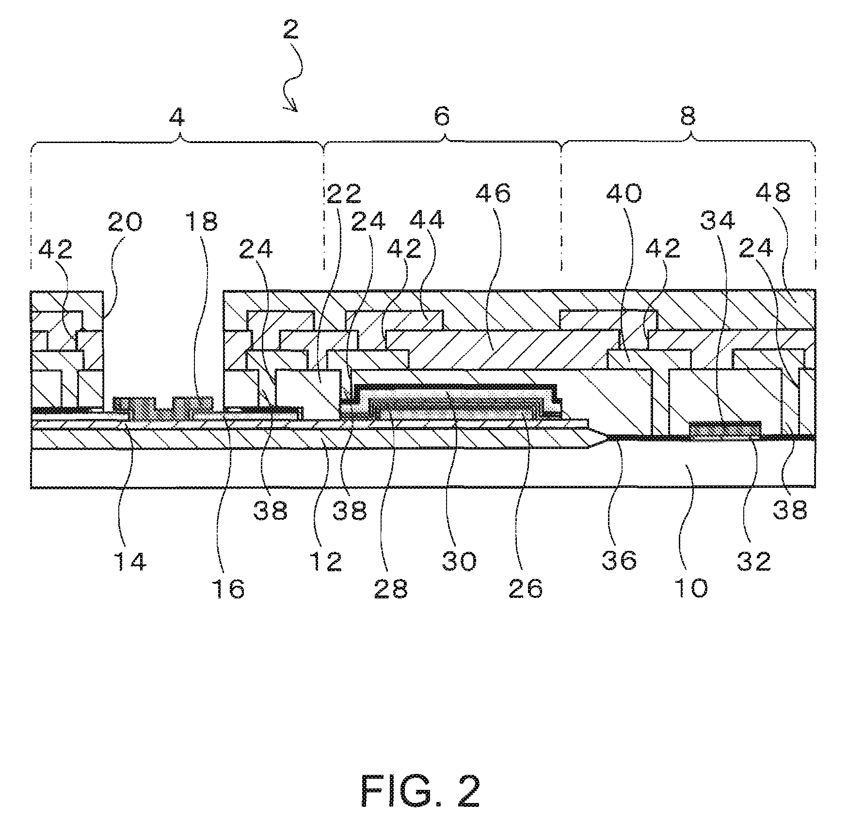
[0019]FIG. 1 is a schematic plan view illustrating a MEMS resonator according to one embodiment to which aspects of the invention are applied. FIG. 2 is a sectional view illustrating a MEMS resonator according to one embodiment to which aspects of the invention are applied. As shown in FIG. 1, the MEMS resonator according to one embodiment of the invention includes a substrate 10, a MEMS structure unit 4 formed on the substrate 10, and a semiconductor device including an ONO capacitor unit 6 and a CMOS circuit unit 8.

[0020]A single-crystal semiconductor substrate may be used as the substrate 10, and examples of materials includes silicon (Si) and gallium arsenide (GaAs). A silicon single-crystal substrate is particularly desirable. The thickness of the substrate 10 ranges from 100 to 1000 μm.

[0021]As shown in FIG. 2, a device isolation oxide film 12 is formed on the...


PUM


Abstract

A method is for manufacturing a microeletromechanical system resonator having a semiconductor device and a microelectromechanical system structure unit formed on a substrate. The method includes: forming a lower electrode of an oxide-nitride-oxide capacitor unit included in the semiconductor device using a first silicon layer; forming, using a second silicon layer, a substructure of the microelectromechanical system structure unit and an upper electrode of the oxide-nitride-oxide capacitor unit included in the semiconductor device; and forming, using a third silicon layer, a superstructure of the microelectromechanical system structure unit and a gate electrode of a complementary metal oxide semiconductor circuit unit included in the semiconductor device.

Description

BACKGROUND[0001]1. Technical Field[0002]The present invention relates to a MEMS resonator and a manufacturing method of the same.[0003]2. Related Art[0004]In recent years, microeletromechanical systems (MEMS) have exhibited a favorable growth in the usage thereof for apparatuses such as acceleration sensors and video devices. There are various interpretations as to what MEMS include conceptually. While in some cases, it is also referred to as “micro machine”, or “micro system technology (MST)”, MEMS generally mean “fine functional devices produced using semiconductor manufacturing techniques”. Those devices are manufactured based on fine processing techniques developed for fabrication of semiconductors. Currently, MEMS are manufactured independently from other manufacturing processes, or, produced onto an integrated circuit (IC) in a process after completing the manufacturing of IC. The field of applications of MEMS includes electric appliances and automobiles, and the field is stil...

Claims


Application Information

Patent Timeline
Patent Type & Authority Patents(United States)
IPC IPC(8): H01L21/66
CPCH03H3/0073H03H9/1057Y10S977/721
Inventor INABA, SHOGOSATO, AKIRAWATANABE, TORUMORI, TAKESHI
Owner SEIKO EPSON CORP
Why Eureka
Try Eureka