High power broadband superluminescent diode

a superluminescent diode and high-power technology, applied in the direction of instruments, semiconductor devices, measurement devices, etc., can solve the problems of limited achievable state separation and spectral bandwidth, devices which cannot achieve high output power and broad optical bandwidth simultaneously, and achieve good thermal and output power performance, and uniform charge injection

Active Publication Date: 2010-03-02
PRAEVIUM RES
View PDF4 Cites 27 Cited by
  • Summary
  • Abstract
  • Description
  • Claims
  • Application Information

AI Technical Summary

Benefits of technology

[0009]The present invention provides a semiconductor-based superluminescent diode in the 1100 nm to 1800 nm region using at least one strained AlGaInAs quantum well grown on an Indium Phosphide substrate. This AlGaInAs quantum well has a deep conduction: valence band offset ratio of approximately 72:28, enabling wide state separation, uniform charge injection, and good thermal and output power performance. A preferred embodiment uses 3 quantum wells in the range of 8-14 nm well width each, providing two quantum confined states with controllable wavelengths, and emitted output power exceeding 50 mW with a bandwidth exceeding 100 nm.
[0010]In one preferred embodiment, each of the AlGaInAs quantum wells has the same composition and thickness, leading to higher output power while maintaining bandwidth in excess of 100 nm. In another preferred embodiment, the well widths are non-uniform to increase spectral range well beyond 100 nm at the expense of reduced gain. In all such multi-quantum well situations, the small valence band offsets of the AlGaInAs material system facilitate controllable wide-bandwidth operation, and high output power and gain due to the large conduction band offset relative to the valence band offset.

Problems solved by technology

This shallow conduction band potential and correspondingly larger valence band potential creates non-uniform charge injection in multi-quantum well structures, reduced thermal and output power performance, particularly in multi-state or non-uniform well width applications, and limited achievable state separation and spectral bandwidth.
The consequence for prior art SLDs has been devices which cannot simultaneously achieve high output power and broad optical bandwidth.
Although this scheme enables broad optical bandwidth, the small fill factor of quantum dot structures leads to limited gain and output power, so high output powers have not thus far been achieved.
Additionally, quantum dot sizes are difficult to control, making center wavelength and bandwidth of quantum dot SLDs unpredictable and un-manufacturable

Method used


Image

  • High power broadband superluminescent diode
  • High power broadband superluminescent diode
  • High power broadband superluminescent diode

Examples


Embodiment Construction

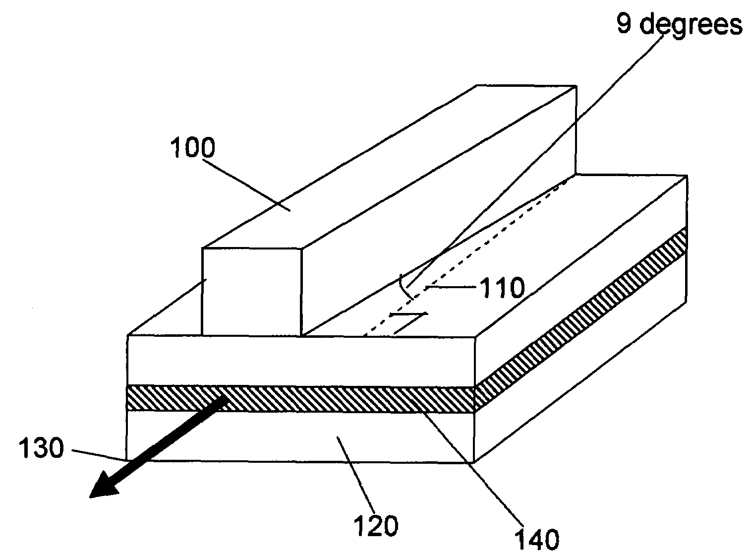
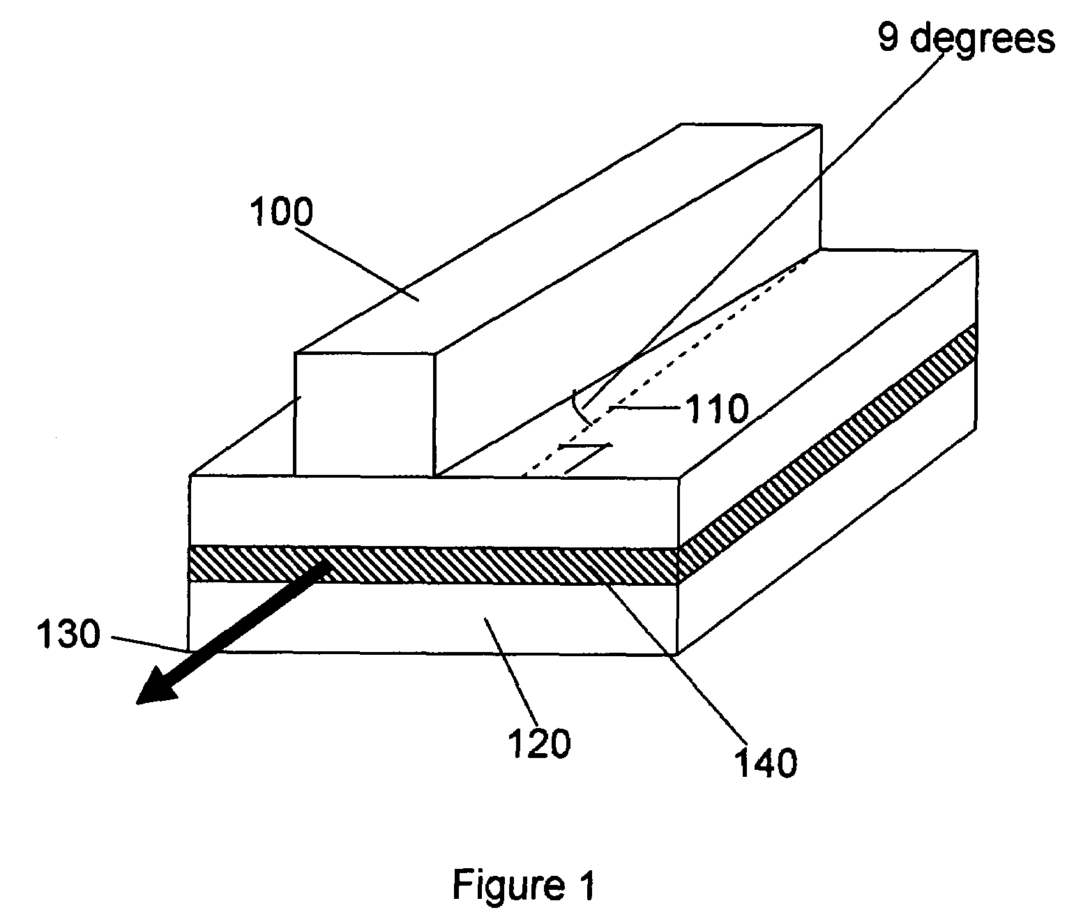
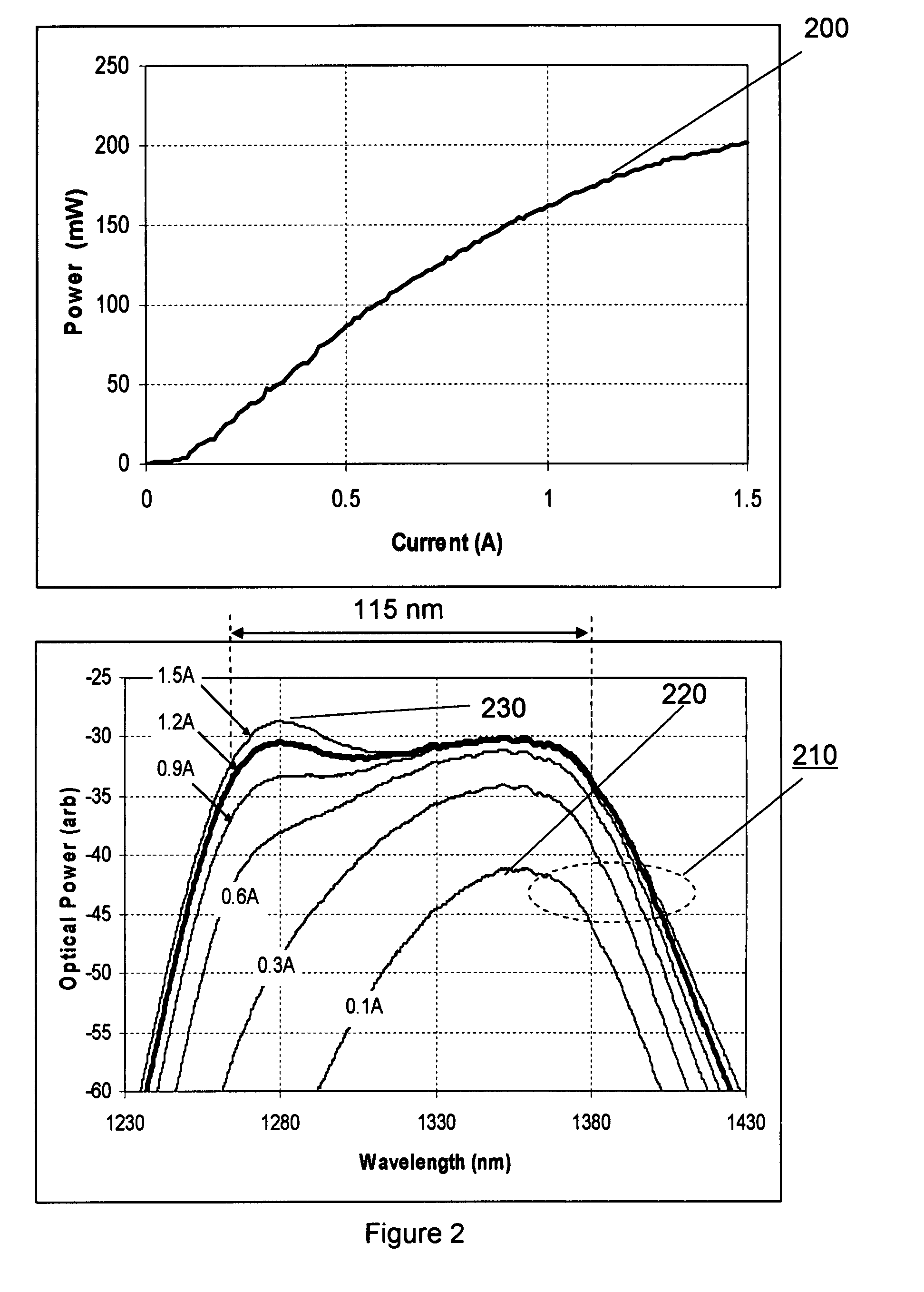
[0040]The present invention provides a superluminescent diode (SLD) on an InP substrate with an AlGaInAs quantum well gain region. FIG. 1 illustrates a preferred embodiment of the present invention, in which a ridge waveguide 100 oriented at about 9 degrees away from a normal 110 to a cleaved facet 120 provides electrical and optical confinement and guides amplified radiation to an output 130. The 9 degree ridge angle effectively suppresses facet reflections and undesired laser action or spectral narrowing. Alternate ridge angles could also be employed without departing from the spirit and scope of the invention as well as other methods for optical guiding and current confinement, such as the use of a buried heterostructure or implantation. Optical gain is provided along the guided region by an AlGaInAs-based quantum well gain region 140 in which both wells and barriers can be defined in composition by parameters x, y in AlyGaxIn1-x-yAs. In the preferred embodiment, light output fro...


PUM


Abstract

A superluminescent diode according the present invention employs a uniform AlGaInAs quantum well on an InP substrate, emitting in a range of 1100 to 1800 nm. The favorable conduction band: valence band offset ratio of this material system enables superluminescent diodes which simultaneously provide high power and large optical bandwidth. A recent reduction to practice of the present invention simultaneously demonstrates output power exceeding 100 mW and bandwidth exceeding 100 nm. A preferred embodiment of this invention uses multiple uniform AlGaInAs quantum wells with two confined quantum states and energetic separation in a range of 100-130 nm. An alternate preferred embodiment uses non-uniform wells, with each well having two confined quantum states. The present invention is particularly useful in time domain and spectral domain optical coherence tomography systems, providing increased resolution and tissue penetration for in-vivo imaging.

Description

CROSS-REFERENCES TO RELATED APPLICATIONS[0001]This application is entiltled to the benefit of Provisional Patent Application Ser. No. 60 / 855,425, filed on Oct. 31, 2006.STATEMENT REGARDING FEDERALLY SPONSORED RESEARCH OR DEVELOPMENT[0002]This invention was made under a government grant 5R44CA101067. The U.S. government has rights in this invention.BACKGROUND-FIELD OF THE INVENTION[0003]This invention relates generally to broadband light sources and superluminescent diodes.BACKGROUND[0004]Semiconductor superluminescent diodes (SLDs) are compact inexpensive light sources for many applications that require large spectral bandwidth. The spectral bandwidth of commercially available SLDs is typically 20-50 nanometers (nm). Many applications would benefit from larger bandwidths. For example, the axial resolution of an optical coherence tomography (OCT) system is effectively the coherence length of the light source, which is inversely proportional to the optical bandwidth of the source. For...

Claims


Application Information

Patent Timeline
Patent Type & Authority Patents(United States)
IPC IPC(8): G01B11/02H01L31/00H01L33/00H01L33/06
CPCG01B9/02H01L33/0045H01L33/06G01B9/02091
Inventor JAYARAMAN, VIJAYSEKHARHALL, ERIC
Owner PRAEVIUM RES
Why Eureka
Try Eureka