Wafer cleaning system

a cleaning system and wafer technology, applied in the direction of cleaning process and apparatus, chemical equipment and processes, semiconductor devices, etc., can solve the problems of ineffective removal of killer particles, inability to eliminate killer particles in the size range of 0.05 to 0.07 micron, and major problems, so as to increase the etch rate of sio2, the effect of increasing the etch ra

Inactive Publication Date: 2010-03-09
LOXLEY TED A
View PDF7 Cites 4 Cited by
  • Summary
  • Abstract
  • Description
  • Claims
  • Application Information

AI Technical Summary

Benefits of technology

[0035]During a SC-1 cleaning process, a cooperative and compensating action exists between the two chemical components. H2O2 oxidizes the silicon and forms a chemical oxide; the formation of this oxide is limited by the diffusion of the oxidizing species. Ammonium hydroxide, conversely, slowly etches this chemically grown oxide. The result of these two processes is that a chemical oxide layer will continually be generated and removed. Particles are thus removed by this etching and undercutting action. Particle removal efficiency can be increased by increasing the etch rate of SiO2. The etch rate, in turn, can be increased by using greater concentrations of NH4OH or by elevating the process temperature.
[0036]The continually increasing integration of advanced IC manufacturing requires tighter process control and specifications. In addition, more stringent environmental requirements are being mandated to reduce chemical and water consumption and waste. The use of megasonic energy has been applied to many wafer surface cleaning procedures as a means to enhance particle removal, reduce chemical concentrations, and shorten process times. The acoustic waves needed for cleaning are about 0.8 to 1.2 MHz and are generated from piezoelectric transducers.

Problems solved by technology

However, such megasonic transducer means was inefficient and ineffective in removing particles with a size smaller than 0.12 micron.
The sub 0.1-micron killer particles left on the wafer surface after cleaning presented a major, major problem.
During the last decade, in the fabrication of advanced devices having a line width or feature size of 0.25 micron, the killer particles in the size range of from 0.05 to 0.07 micron, for example, that could not be eliminated by megasonic means, were particularly troublesome.
The use of sophisticated chemical treatments or other special measures combined with the best available megasonic means was highly advantageous but not an ideal or complete solution to the particulate contamination problem.
It was manifest to everyone that the known megasonic wafer cleaning systems were deficient and inadequate for manufacture of the more advanced microelectronic devices, such as those having a line width or feature size of 0.10 micron or less and also that extensive research would be needed to solve the seemingly impossible particle contamination problem.
In recent years, researchers came to realize that the use of excessive megasonic energy during the fabrication process was risky and could degrade the microcircuits and cause them to be unreliable, and that serious defects would often be undetectable.
It has so far been unsuccessful.
The foremost experts in the field concluded that megasonic systems or other wet wafer cleaning systems were not promising, that they provided no practical way to remove or eliminate sub 0.1-micron killer particles, and that the semi-conductor industry would have to develop more sophisticated dry wafer cleaning processes.
Heretofore the semiconductor industry believed that wet cleaning methods would never be effective in removing adhered colloidal-size contaminant particles.
On this basis the best scientific minds grappling with the problem including foremost experts, such as Werner Kern, concluded that wet cleaning processes could not provide a satisfactory way to remove colloidal-size particles when manufacturing the most advanced microchips and that the only real hope for success was a breakthrough or major improvement in dry wafer cleaning technology.

Method used


Image

  • Wafer cleaning system
  • Wafer cleaning system
  • Wafer cleaning system

Examples


Embodiment Construction

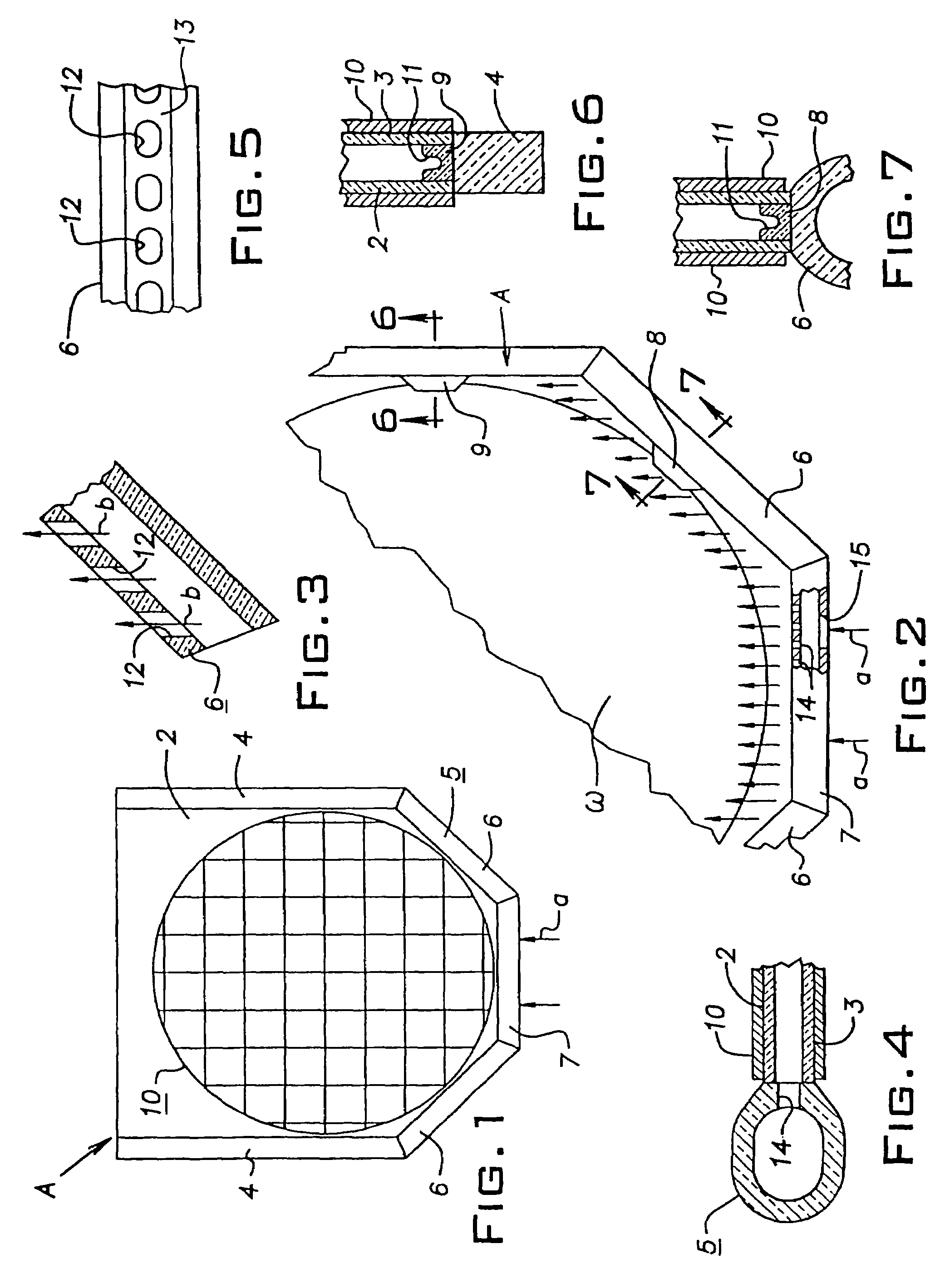
[0161]One of the embodiments of the present invention is illustrated in FIGS. 1 to 7 and employs a flattened wafer holder and receptacle 10 designed to receive a single semiconductor wafer w. This embodiment and other embodiments of a similar nature using single-wafer receptacles or the like are believed well suited for modern fabrication systems, particularly those that employ silicon wafers with diameters of 200 mm or more.

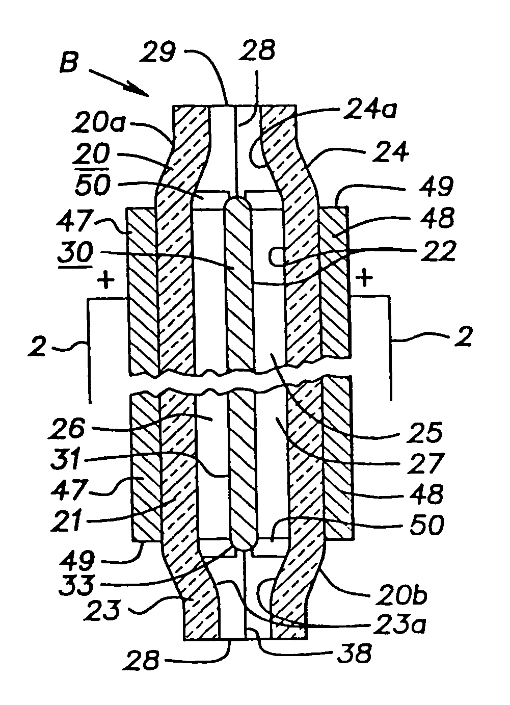
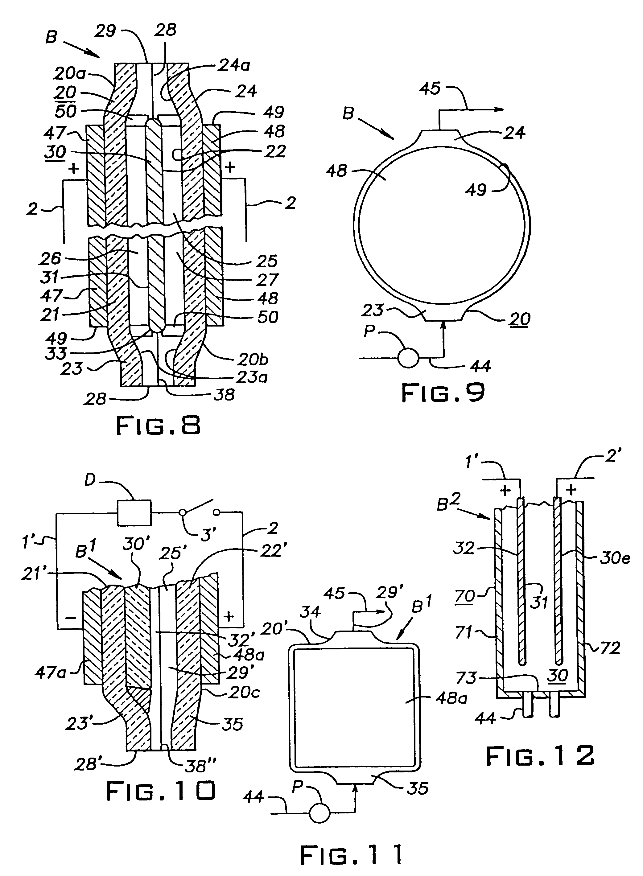
[0162]FIGS. 1 to 7 illustrate an embodiment of the present invention wherein a wafer carrier formed of glass, silicon or other suitable material has a narrow internal cavity that receives a single silicon semiconductor wafer and has means for charging the wafer to a small voltage during wet processing operations. These figures provide a simple schematic illustration of apparatus particularly well suited for use in the practice of the invention and are intended to facilitate a ready understanding of the invention and the various ways the apparatus can be used in ...


PUM

PropertyMeasurementUnit
distanceaaaaaaaaaa
voltageaaaaaaaaaa
diameteraaaaaaaaaa

Abstract

An electromegasonic wafer cleaning system is disclosed that is extremely important, if not essential, in the fabrication of advanced microelectronic devices having a line width or feature size of from 0.05 to 0.10 micron. A unique synergistic combination is provided wherein piezoelectric transducer means are operated at a tolerable power level, such as from 1 to 2 watts per square centimeter, to minimize the risk of harm to the extremely delicate microcircuits and wherein the face of each wafer is negatively charged to a temperate voltage, such as from 5 to 20 volts, sufficient to cause effective removal of colloidal or sub 0.4-micron contaminant particles.
This unique wafer cleaning system supersedes and replaces the standard megasonic-assisted RCA-type wet wafer cleaning systems which have never been able to eliminate or provide efficient purging of harmful sub 0.1-micron particles.

Description

[0001]This application is a continuation-in-part of application Ser. No. 09 / 490,162 filed on Jan. 22, 2000, now abandoned and contains divisional subject matter.[0002]The invention as shown and described herein relates to the cleaning of semiconductor wafers in the manufacture of microprocessors, integrated circuits, and other sophisticated electronic devices. The invention involves the discovery of a seemingly simple and very effective wet cleaning system that can substantially eliminate colloidal or sub 0.05-micron particles during the fabrication and processing of semiconductor wafers.[0003]A preferred embodiment of the invention relates to a simple and unique cleaning apparatus comprising a special shaped receptacle designed for a single silicon wafer.[0004]This invention provides a superb electromegasonic wafer cleaning system that may be indispensable or vitally important in the fabrication of the most advanced microelectronic devices. The remarkable synergistic combination of...

Claims


Application Information

Patent Timeline
Patent Type & Authority Patents(United States)
IPC IPC(8): H01L21/04
CPCH01L21/02057H01L21/67057H01L21/67303Y10S438/906
Inventor LOXLEY, TED A.
Owner LOXLEY TED A
Why Eureka
Try Eureka