Optoelectronic integrated circuit board and communications device using the same

an optoelectronic integrated circuit and optical coupling technology, applied in the direction of optical elements, instruments, semiconductor lasers, etc., can solve the problems of increasing the number of wirings and the seriousness of crosstalk between wirings, and achieves high refractive index, suppressed light beam spread, and high accuracy positioning of optical devices

Inactive Publication Date: 2010-03-16
RESONAC CORPORATION
View PDF12 Cites 27 Cited by
  • Summary
  • Abstract
  • Description
  • Claims
  • Application Information

AI Technical Summary

Benefits of technology

[0014]The present invention enables highly accurate positioning of an optical device arranged on the top surface of the multilayered optical waveguide unit by positioning of a mirror arranged in the core having a high refractive index provided in an optical waveguide. Furthermore, light propagated to the second and subsequent optical waveguide layers is from an upper optical waveguide via a core having a high refractive index provided in the upper optical waveguide layer, so that spread of the light beam is suppressed with lowering of the optical coupling efficiency prevented, and furthermore a light path of a light beam propagating through the core is changed and guided to an optical device provided on a top surface of the board, so that a required space can be ensured between the optical devices, which allows for high density integration of optical wirings and prevention of cross talk between the wirings. Furthermore, the present invention advantageously provides an optoelectronic integrated circuit board which allows for reduction of required components and manufacturing processes and also enables cost reduction.

Problems solved by technology

Furthermore, the high-frequency lines need a waveform shaping circuit and require countermeasures against such problems as reflection and crosstalk between the wirings.
Because there is the tendency for growth in system capacity, it is anticipated that the problems including increase of the number of wirings and crosstalk between wirings will become more serious in a device using the conventional electric wirings for processing a large volume of information at a processing speed of T bit / s or more.

Method used


Image

  • Optoelectronic integrated circuit board and communications device using the same
  • Optoelectronic integrated circuit board and communications device using the same
  • Optoelectronic integrated circuit board and communications device using the same

Examples


first embodiment

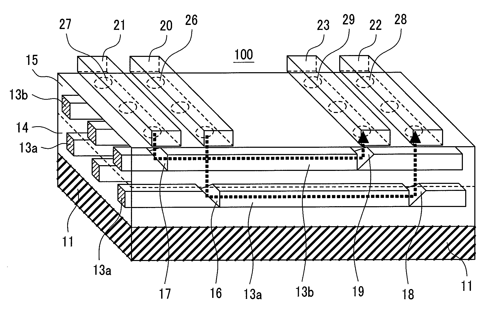
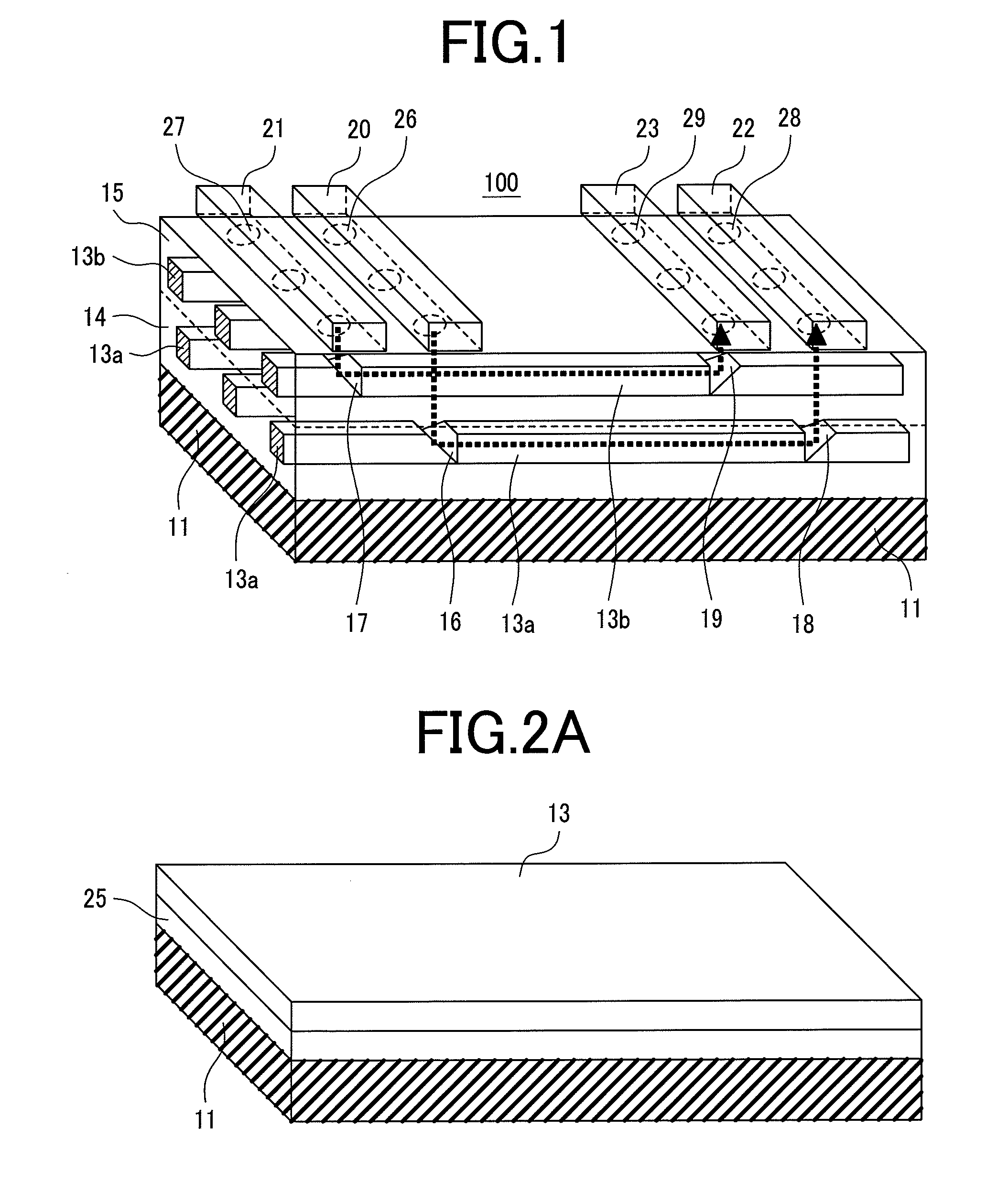
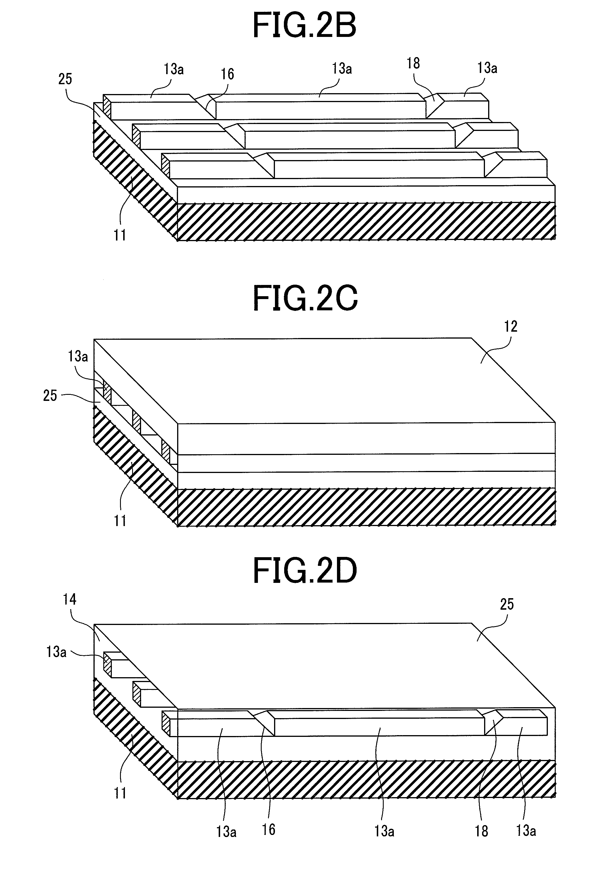
[0015]FIG. 1 is a perspective view illustrating an optoelectronic integrated circuit board 100 according to a first embodiment of the present invention. A board 11 is prepared with glass epoxy, ceramics, and the like. A configuration of the board 11 is two-layered and includes a first optical waveguide layer 14 having a plurality of cores 13a each having a high refraction index and embedded by a cladding layer, and a second optical waveguide layer 15 formed on the first optical waveguide layer having a plurality of cores 13b each having a high refractive index and embedded by a cladding layer, the first and second optical waveguide layers arranged on the substrate 11. The core 13a and the core 13b are positioned at the same position in the vertical direction. Mirrors 16 and 18, and mirrors 17 and 19 are arranged in the cores 13a and 13b which are respectively included in the optical waveguide layers 14 and 15. As illustrated in the figure, reflection surfaces of the mirrors 16 and 1...

second embodiment

[0028]FIG. 4 is a perspective view illustrating an optoelectronic integrated circuit board 200 according to a second embodiment of the present invention. In the optoelectronic integrated circuit board 200, different from the optoelectronic integrated circuit board 100, the mirrors 16, 18 of the core 13a located at a position further from a top surface of the optoelectronic integrated circuit board 200 and the core 13b through which light passes when transmitted and received to and from an optical device on the top surface of the optoelectronic integrated circuit board 200 are separated and isolated from each other in each light path. Because of the configuration, propagated light in the vertical direction is more tightly blocked in the separated and isolated isolation cores 13b1, 13b2, which enables realization of highly efficient optical coupling performance. Also in this embodiment, a path of light propagated through the cores 13a, 13b is represented by a broken line like in FIG. ...

third embodiment

[0034]FIG. 7 is a cross-sectional view illustrating a optoelectronic integrated circuit board 300 according to a third embodiment of the present invention. In the example shown in FIG. 7, a two-layered optical waveguide comprising a first optical waveguide 14 and a second optical waveguide 15 is laminated on a substrate 11 like in the first and second embodiments described above, and then a third optical waveguide 40 is laminated on the two-layered optical waveguide by the same technique as described in relation to FIG. 2E, and FIG. 2F. In the third optical waveguide layer 40, a core 13c, mirrors 41 and 42, a tapered isolated cores 13c1, 13c2, 13c3 and 13c4 each separated from the core 13c are formed. These components can be formed by the same technique as that employed for preparing the tapered and isolated cores 13b1 and 13bs separated from the core 13 in the second optical waveguide. The mirror 16 in the optical waveguide layer 40, the separated and isolated tapered core 13b1 of ...


PUM


Abstract

In the optical connection between multi-layered optical waveguides and photoelectric converting elements or optical waveguide array connectors formed on a substrate, the optical coupling efficiency is to be prevented from degrading due to deviation of the optical axis positions between optical elements and the optical waveguide layers that is caused by a radiation due to a beam expansion or by a deviation of positioning layers in producing the optical waveguides. There are stacked, on a substrate, optical waveguide layers, each of which comprises a clad layer and a core having a higher refractive index than the clad layer, and optical elements formed on the uppermost optical waveguide layer. The optical elements are positioned such that they correspond to the optical path conversion mirrors of the cores of the underlaying optical waveguide layer. The light transmission / reception between the optical elements and the optical path conversion mirrors of the cores of the underlaying optical waveguide layer is performed via the cores of overlying optical waveguide layer.

Description

TECHNICAL FIELD[0001]The present invention relates to an optical wiring structure and an optical coupling system of an optoelectronic integrated circuit capable of processing high-capacity optical signals transmitted and received between substrates in a communication device and a communication device using the circuit.BACKGROUND ART[0002]Currently, in the field of information processing and telecommunications, an improvement of communication traffics communicating high-capacity data using the optical technology is rapidly progressing, and there have been developed optical fiber networks such as a backbone, Metro, and Access for long distances of a few kilometers and more. It would be effective in the future to use optical wirings for processing a large volume of data without delay for signal transmission between communication devices (over the distance from several meters to several hundreds meters), and even for communications over an extremely short distance (in the range from sev...

Claims


Application Information

Patent Timeline
Patent Type & Authority Patents(United States)
IPC IPC(8): G02B6/42G02B6/122G02B6/30H01L31/0232H01L33/08H01L33/48H01L33/60H01S5/022H05K1/02
CPCG02B6/43G02B6/4214H05K1/0274
Inventor MATSUOKA, YASUNOBUSHISHIKURA, MASATO
Owner RESONAC CORPORATION
Why Eureka
Try Eureka