Bismuth ferrite films and devices grown on silicon

a technology of bismuth ferrite and silicon, which is applied in the direction of microstructural devices, microstructured devices, transistors, etc., can solve the problems of introducing reliability problems in semiconductor circuits, presenting difficulties in using pzt as the functional metal oxide layer, and raising environmental issues

Inactive Publication Date: 2010-04-13
MARYLAND UNIV OF
View PDF6 Cites 16 Cited by
  • Summary
  • Abstract
  • Description
  • Claims
  • Application Information

AI Technical Summary

Problems solved by technology

One of the challenges of commercially important ferroelectric memories addressed in the above cited patent is integrating a large number of such ferroelectric cells on a silicon substrate.
Again, the challenge is to integrate onto a silicon substrate a significant number of such devices including the piezoelectric layer.
The use of PZT as the functional metal oxide layer presents some difficulties.
Lead is toxic and thus raises environmental issues both during fabrication and for disposal of old devices.
Furthermore, lead is considered a heavy metal contaminant in the fabrication of silicon integrated circuits and it may introduce reliability problems in semiconductor circuits.

Method used


Image

  • Bismuth ferrite films and devices grown on silicon
  • Bismuth ferrite films and devices grown on silicon
  • Bismuth ferrite films and devices grown on silicon

Examples


Embodiment Construction

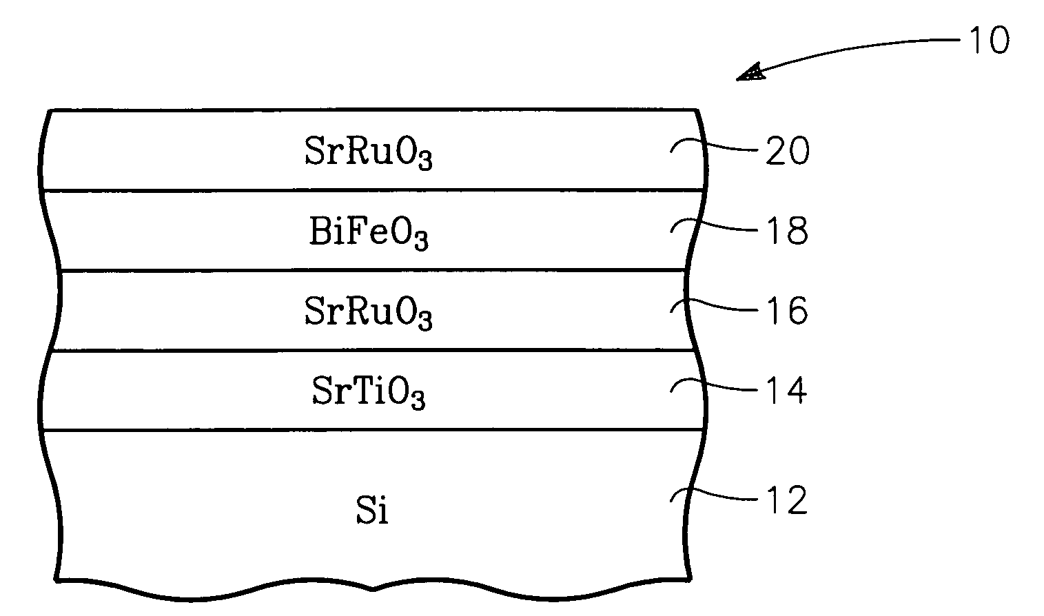
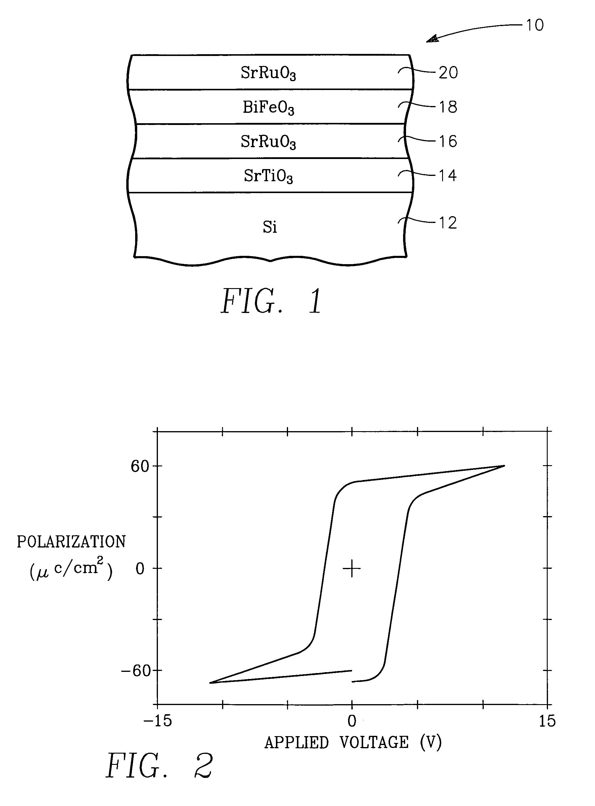
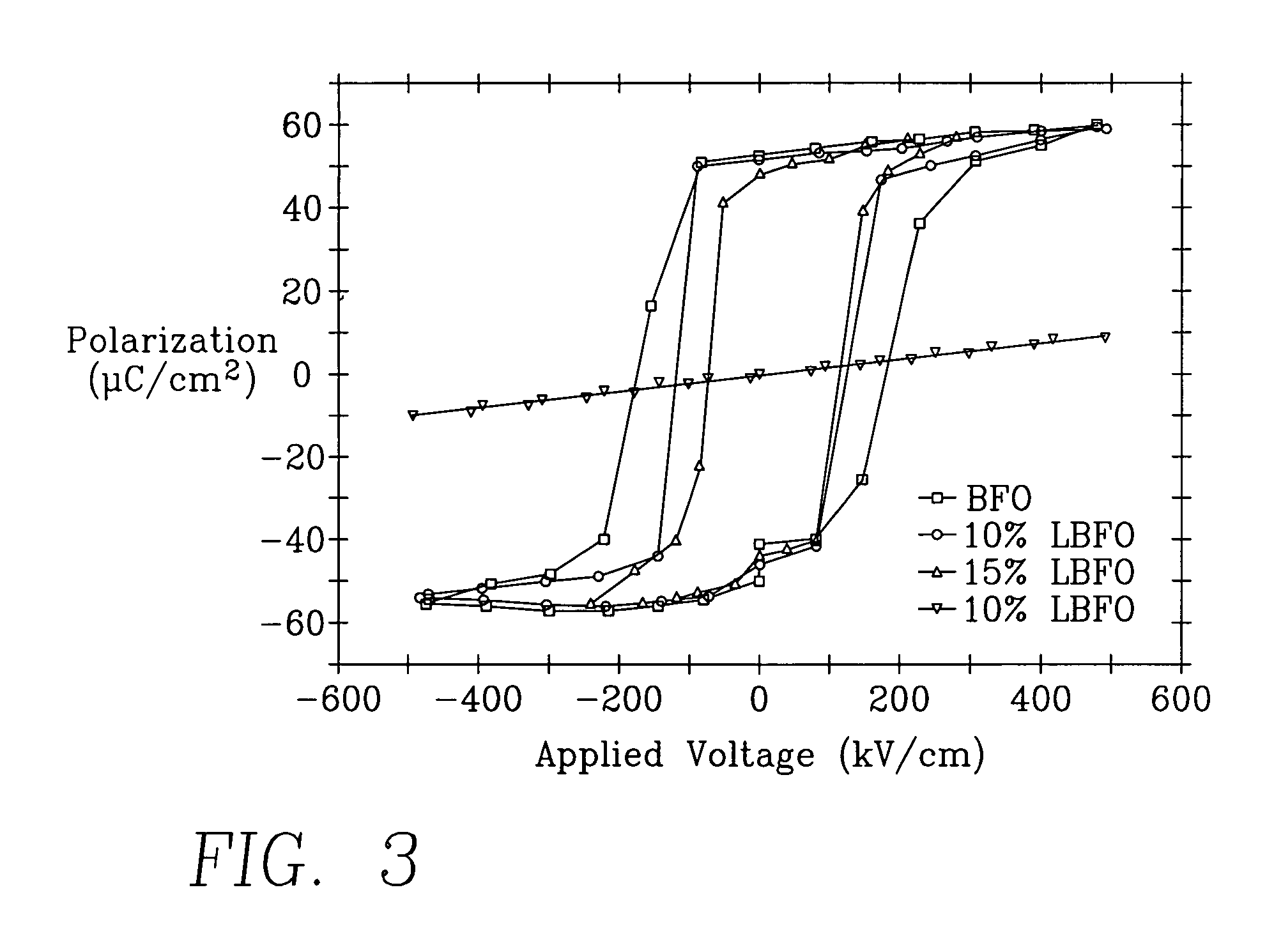
[0026]The perovskite material bismuth ferrite (BiFeO3 or BFO), also called bismuth iron oxide, can be substituted for PZT and related materials as the functional metal oxide layer in many commercially important devices. The class may be expanded to cover cationically substituted derivatives of BFO, for example, by substituting lanthanum or similar rare-earth elements. The indicated composition of BiFeO3 need not be precise or exactly stoichiometric, as is well known. The perovskite material may also be a cationically substituted derivative of BFO, such as La-substituted BFO. In the bulk, BFO is known to exhibit a rhombohedrally distorted perovskite crystal structure with rhombohedral unit cell parameters of cell length α=0.56166 nm and angle α=59.355° and a psuedo-cubic unit lattice of about 0.396 nm. BFO also exhibits a good ferroelectric effect with a high Curie temperature TC of about 825° C. and some anti-ferromagnetism with a Neel temperature TN of about 400° C. Recent measurem...


PUM

PropertyMeasurementUnit
thicknessaaaaaaaaaa
cell lengthaaaaaaaaaa
Neel temperature TNaaaaaaaaaa

Abstract

A functional perovskite cell formed on a silicon substrate layer and including a functional layer of bismuth ferrite (BiFeO3 or BFO) sandwiched between two electrode layers. An optional intermediate template layer, for example, of strontium titanate allows the bismuth ferrite layer to be crystallographically aligned with the silicon substrate layer. Other barrier layers of platinum or an intermetallic alloy produce a polycrystalline BFO layer. The cell may be configured as a non-volatile memory cell or a MEMS structure respectively depending upon the ferroelectric and piezoelectric character of BFO. Lanthanum substitution in the BFO increases ferroelectric performance. The films may be grown by MOCVD using a heated vaporizer.

Description

RELATED APPLICATION[0001]This application is a continuation in part of U.S. patent application Ser. No. 11 / 197,532, filed Aug. 4, 2005, incorporated herein by reference.FIELD OF THE INVENTION[0002]The invention relates generally to oxide thin film and devices formed thereby. In particular, the invention relates to thin films having a perovskite crystal structure and being ferroelectric or magnetic and / or exhibiting an interaction with other parameters such as piezoelectricity.BACKGROUND ART[0003]There has been much recent interest and development in electronic devices incorporating a functional metal oxide layer. Perovskite thin films are particularly useful because many perovskite materials exhibit non-linear behavior such as ferroelectricity or have electrical characteristics that depend on other parameters such that they can be used for sensors or actuators.[0004]One such application is a non-volatile ferroelectric memory as I have described in U.S. Pat. No. 6,518,609, incorporat...

Claims


Application Information

Patent Timeline
Patent Type & Authority Patents(United States)
IPC IPC(8): H01L29/72
CPCB81B3/0018H01L21/31691H01L28/56H01L27/11507H01L27/11502H01L21/02194H01L21/02203H10B53/30H10B53/00
Inventor RAMESH, RAMAMOORTHY
Owner MARYLAND UNIV OF
Why Eureka
Try Eureka