Single-shot semiconductor processing system and method having various irradiation patterns

a semiconductor and processing system technology, applied in the field of single-shot semiconductor processing system and method having various irradiation patterns, can solve the problems of insufficient ela process, amorphous or polycrystalline, and the general proportional deformation of the device characteristics of the tft fabricated in the silicon thin film, etc., to achieve the effect of improving the crystalline quality, facilitating the processing of large surface area semiconductor thin films, and being suitable for device applications

Inactive Publication Date: 2010-05-18
THE TRUSTEES OF COLUMBIA UNIV IN THE CITY OF NEW YORK
View PDF268 Cites 1 Cited by
  • Summary
  • Abstract
  • Description
  • Claims
  • Application Information

AI Technical Summary

Benefits of technology

[0007]The present invention provides systems and methods for recrystallizing amorphous or polycrystalline semiconductor thin films to improve their crystalline quality and to thereby make them more suitable for device applications. The systems and processes are designed so that large surface area semiconductor thin films can be processed quickly.

Problems solved by technology

The relatively low deposition temperatures degrade the crystallinity of the deposited silicon films and cause them to be amorphous or polycrystalline.
Unfortunately, the device characteristics of a TFT fabricated in a silicon thin film undesirably degrade generally in proportion to the non-crystallinity of the silicon thin film.
The conventional ELA processes, however, are not entirely satisfactory at least in part because the grain sizes in the annealed films are not sufficiently uniform for industrial use.

Method used


Image

  • Single-shot semiconductor processing system and method having various irradiation patterns
  • Single-shot semiconductor processing system and method having various irradiation patterns
  • Single-shot semiconductor processing system and method having various irradiation patterns

Examples


Embodiment Construction

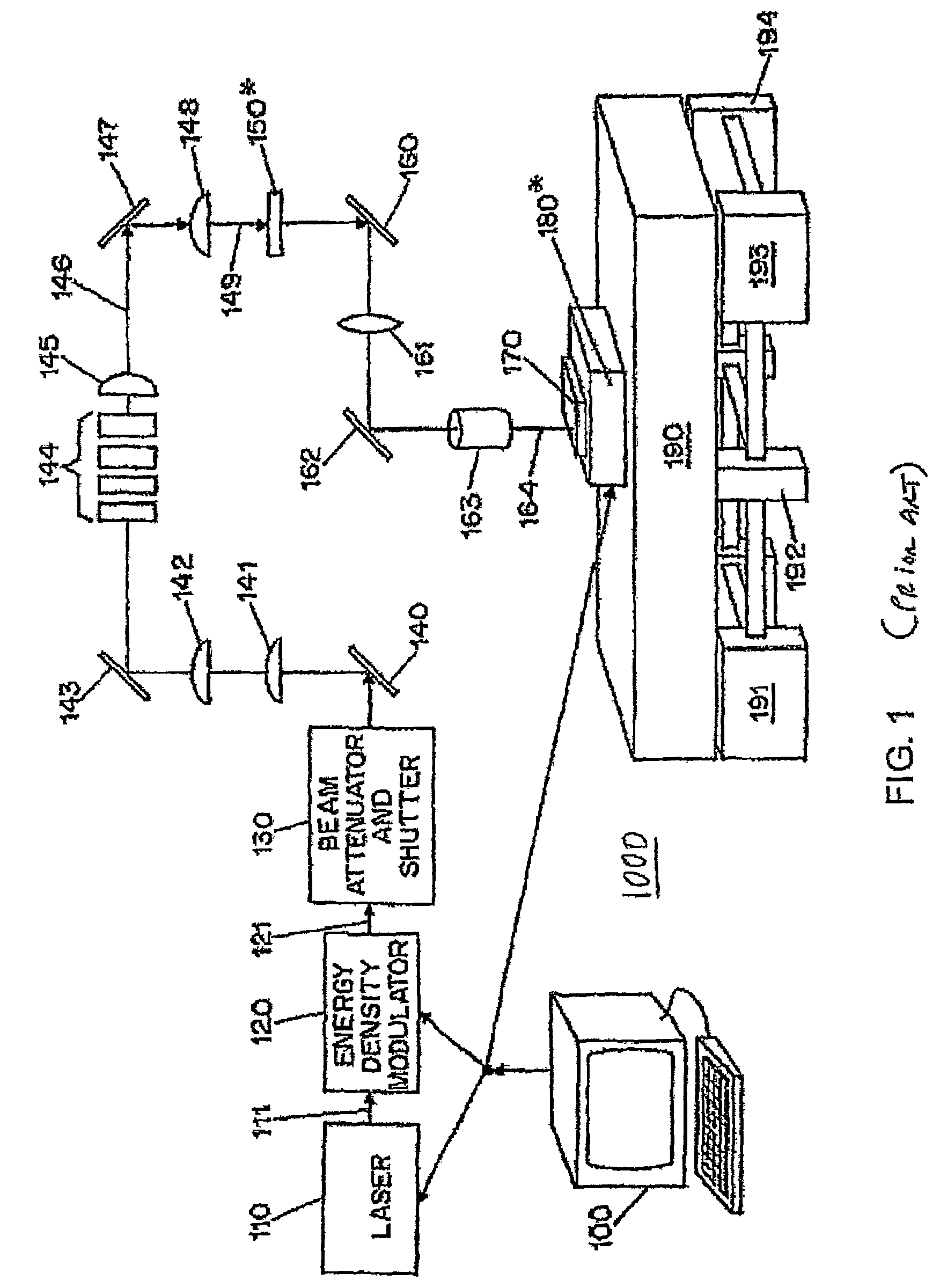
[0020]The present invention provides processes and systems for recrystallization of semiconductor thin films by laser annealing. The processes for recrystallization of semiconductor thin films involve one-shot irradiation of regions of a semiconductor thin film workpiece to a laser beam. The systems direct a laser beam to a region or spot on the surface of the semiconductor thin film. The incident laser beam has sufficient intensity or fluence to melt targeted portions of the region or spot of the semiconductor thin film on which the laser beam is incident. After the targeted incident areas or portions are melted, the laser beam is moved or stepped to another region or spot on the semiconductor thin film. The molten semiconductor material recrystallizes when the incident laser beam is moved away. The dwell time of the laser beam on a spot on the semiconductor thin film may be sufficient small so that the recrystallization of an entire semiconductor thin film workpiece can be carried...


PUM

PropertyMeasurementUnit
thicknessaaaaaaaaaa
thicknessaaaaaaaaaa
crystalline qualityaaaaaaaaaa

Abstract

High throughput systems and processes for recrystallizing thin film semiconductors that have been deposited at low temperatures on a substrate are provided. A thin film semiconductor workpiece is irradiated with a laser beam to melt and recrystallize target areas of the surface exposed to the laser beam. The laser beam is shaped into one or more beamlets using patterning masks. The mask patterns have suitable dimensions and orientations to pattern the laser beam radiation so that the areas targeted by the beamlets have dimensions and orientations that are conducive to semiconductor recrystallization. The workpiece is mechanically translated along linear paths relative to the laser beam to process the entire surface of the work piece at high speeds. Position sensitive triggering of a laser can be used generate laser beam pulses to melt and recrystallize semiconductor material at precise locations on the surface of the workpiece while it is translated on a motorized stage.

Description

CROSS-REFERENCE TO RELATED APPLICATION[0001]This application is a national phase of Internation Patent Application No. PCT / US03 / 025947, filed Aug. 19, 2003, published on Feb. 26, 2004 as International Patent Publication No. WO 04 / 017380, which claims priority from U.S. patent application No. 60 / 404,447, filed on Aug. 19, 2002, each of which are incorporated by reference in their entireties herein, and from which priority is claimed.BACKGROUND OF THE INVENTION[0002]The present invention relates to semiconductor processing methods, and more particularly, to methods for making semiconductors materials in a form suitable for fabrication of thin-film transistor (“TFT”) devices.[0003]Flat panel displays and other display units are used as visual imaging interfaces for the common and ubiquitous electronic devices and appliances such as computers, image sensors, and television sets. The displays are fabricated, for example, from thin films of liquid crystal and semiconductor material placed...

Claims


Application Information

Patent Timeline
Patent Type & Authority Patents(United States)
IPC IPC(8): H01L21/00H01L21/20
CPCB23K26/0656H01L21/2026H01L27/1285H01L21/324H01L21/02675H01L21/02H01L27/1296Y10T117/1088Y10T117/10B23K26/066H01L21/02422H01L21/02686H01L21/02678H01L21/02532
Inventor IM, JAMES S.
Owner THE TRUSTEES OF COLUMBIA UNIV IN THE CITY OF NEW YORK
Why Eureka
Try Eureka