Eureka AIR delivers breakthrough ideas for toughest innovation challenges, trusted by R&D personnel around the world.

Fourier filters, systems for fabricating fourier filters, and systems and methods for inspecting a specimen using fourier filters

Active Publication Date: 2010-06-15
KLA TENCOR CORP
View PDF9 Cites 5 Cited by
  • Summary
  • Abstract
  • Description
  • Claims
  • Application Information

AI Technical Summary

Benefits of technology

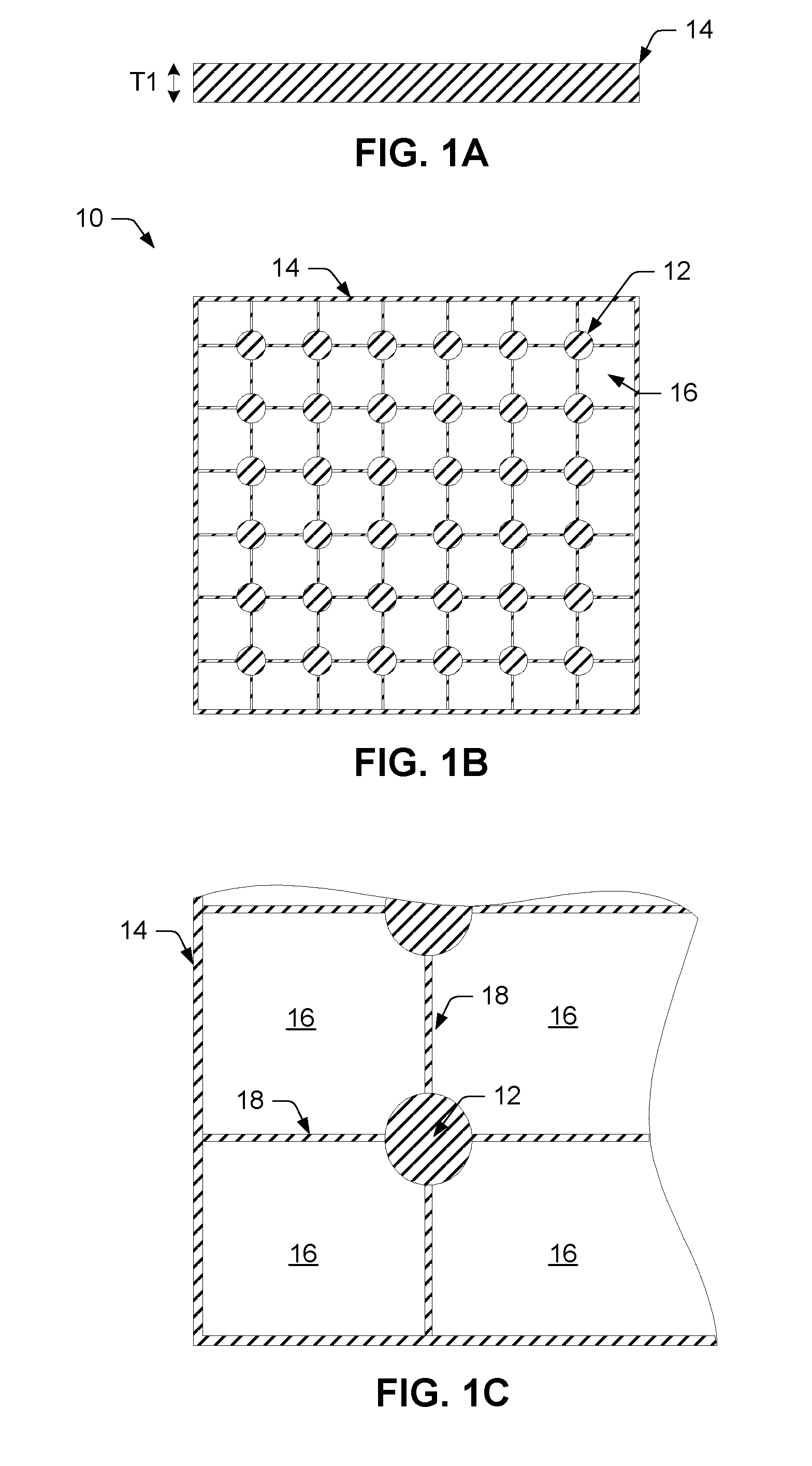
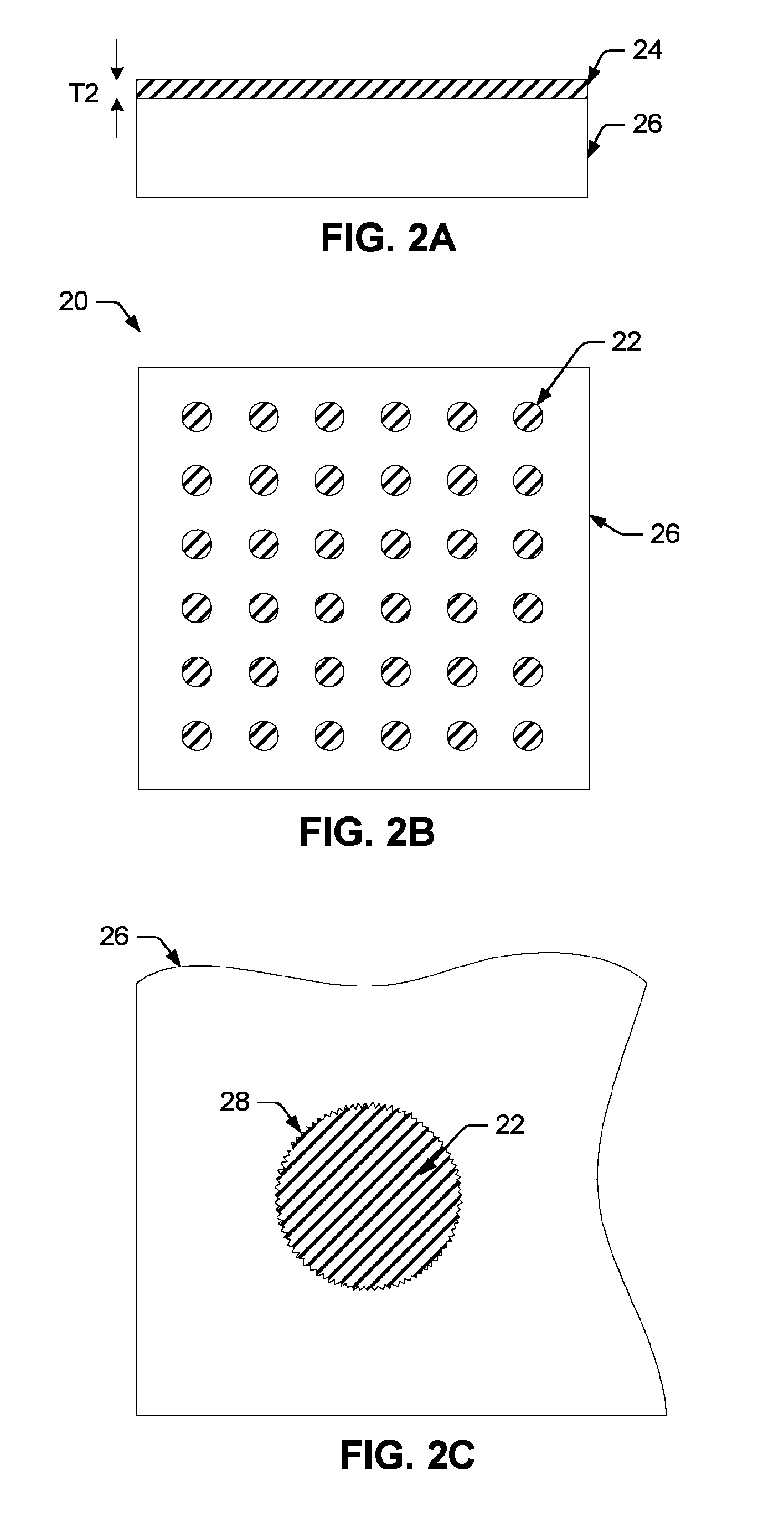
[0020]In general, the select portions of the optically opaque layer may be removed, such that each of the patterned features in the array includes an optically opaque center portion surrounded by at least one transmissive region. In some embodiments, a shape of the optically opaque center portion may be substantially circular. However, the optically opaque center portion is not limited to a circular shape in all embodiments of the invention. In other embodiments, the shape of the optically opaque center portion may be substantially different from circular depending on the optical aberrations, flare and ghosting of the system, as well as the surface roughness the sample. In particular, the Fourier filter design may be based on images obtained from the Fourier plane. Regardless of the particular filter design, the optically opaque center portion may be formed with rough edges, in some embodiments of the invention, to reduce any ringing that may be induced by the Fourier filter.
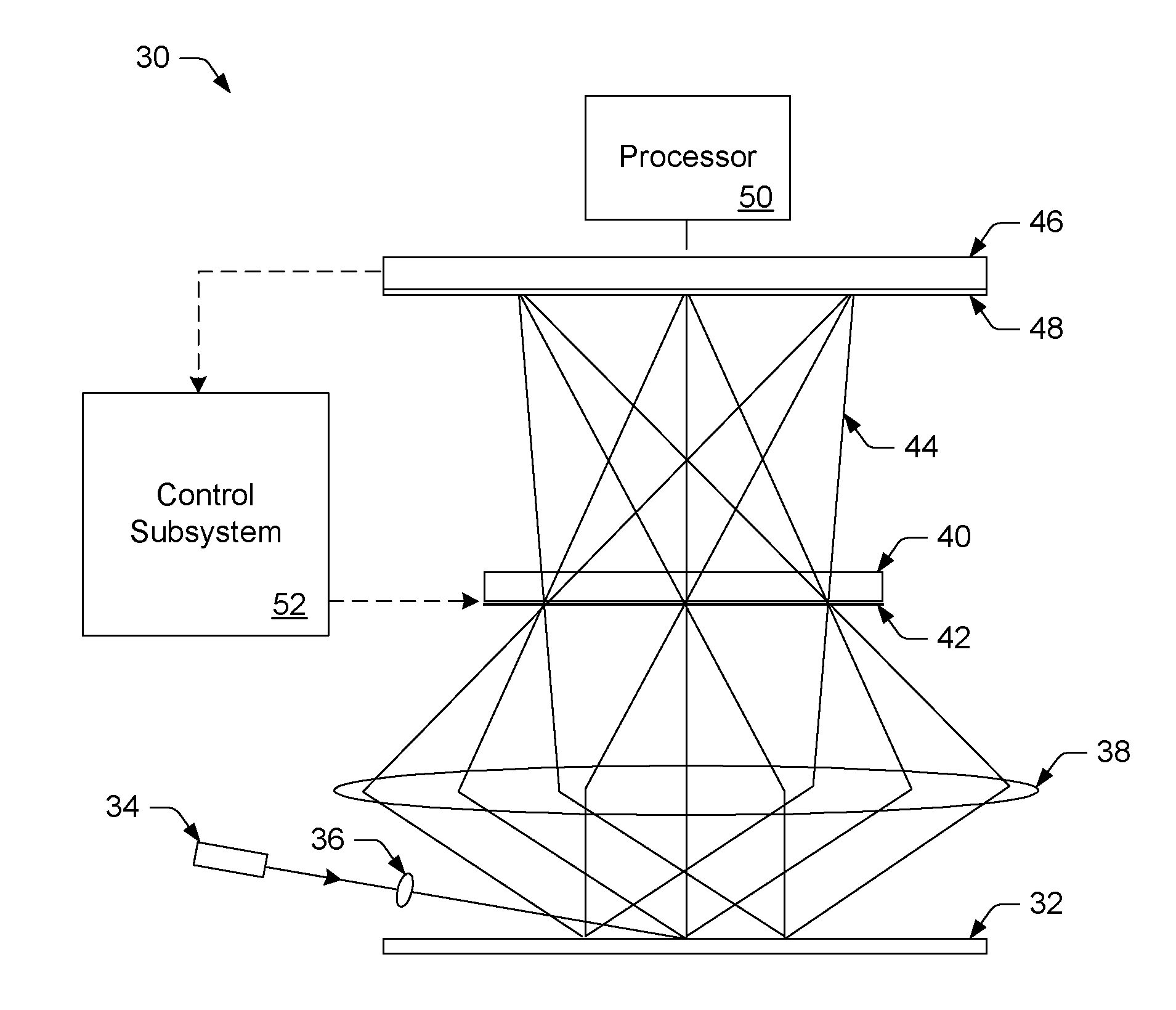
[0025]The system may also include a Fourier filter positioned at a Fourier plane of the collection subsystem. As noted above, the Fourier filter may include an array of patterned features formed within an optically opaque layer. The array of patterned features may be configured to block light reflected and diffracted from structures on the specimen and to allow light scattered from defects on the specimen to pass through the filter to the detection subsystem of the system. The array of patterned features may be formed as described further herein. For example, the array of patterned features may be formed by removing portions of the optically opaque layer to create transmissive regions, which only allow the light scattered from the defects to pass through. Positioning the Fourier filter within the Fourier plane of the inspection system enables the detection subsystem to generate output responsive to light passed through the transmissive regions, so that the output can be used for detecting the defects on the specimen.
[0027]In some embodiments, the fabrication subsystem may generally include a holder and a laser. The holder may be configured to align the optically opaque layer within the fabrication subsystem. The laser may be configured to form the array of patterned features by removing select portions of the optically opaque layer under control of the control subsystem. As noted above, the select portions removed by the laser may only allow light scattered from defects on the specimen to pass through the Fourier filter. As such, the Fourier filter formed by the fabrication subsystem may enable defects to be detected more easily.
[0031]In other embodiments, the method may inspect the specimen for defects by using a custom mask to filter light reflected and diffracted from periodic structures on the specimen. For example, a custom mask may be fabricated “on the fly” (i.e., during the inspection process) to block light reflected and diffracted from the periodic structures on the specimen and to allow light scattered from defects on the specimen to pass through. The method may choose to fabricate the custom mask if the diffraction pattern is unknown prior to the step of illuminating and a predetermined mask is unavailable or otherwise unsuitable for the inspection process. The custom mask may comprise any of the Fourier filter embodiments described herein and may be fabricated in accordance with any of the fabrication processes described herein. As such, the custom mask may be fabricated relatively quickly (e.g., within minutes) and with relatively little cost.
[0032]In general, the custom mask may be fabricated by generating an image of light in a Fourier plane of the inspection system, where the image comprises light reflected and diffracted from the structures on the specimen. The generated image (i.e., an image of the diffraction pattern) may then be used to fabricate the custom mask. For example, the image may be used to form an array of patterned features within an optically opaque layer, such as a relatively thin sheet of metal, a relatively thin sheet of plastic or a relatively thin layer of metal formed upon an optically transmissive substrate. In some embodiments, the array of patterned features may be formed by removing select portions of the optically opaque layer with laser light. As noted above, the select portions may only allow the light scattered from defects on the specimen to pass through the custom mask. As such, the custom mask formed by the method may enable defects to be detected more easily.

Problems solved by technology

Inspection tools for unpatterned wafers are generally not capable of inspecting patterned wafers for a number of reasons.
In some cases, unpatterned wafers, or “monitor wafers,” which have been run through a process tool, may be inspected as a gauge for the number and types of defects that may be found on patterned wafers, or “product wafers.” However, the defects detected on monitor wafers do not always accurately reflect the defects that are detected on product wafers after the same process in the same process tool.
Although the mechanical method is widely used, it has a number of disadvantages, particularly for flood illumination based inspection systems.
In addition, the mechanical method induces significantly more Fourier filter ringing, which reduces defect sensitivity.
For example, Fourier filters in the form of periodic blocking bars diffract light into undesirable directions, inducing “ringing” or side lobes in the defect signals.
In some cases, the side lobes may produce significant distortion at the image plane of the inspection system, adversely affecting the ability of the inspection system to detect defects on the wafer with high accuracy.
As such, only a limited number of rods can be used; otherwise, the entire plane would be blocked by the rods.
However, there are several factors that make liquid crystal devices inappropriate for flood illumination based inspection systems.
However, light scattering significantly alters the wavefront of the inspection system, causing severe degradation to the image quality.
In addition, most liquid crystal material has a damage threshold at a wavelength of approximately 300 nm, making liquid crystal devices less than ideal for use in deep ultraviolet (DUV) based systems (i.e., systems that operate at wavelength(s) less than about 300 nm).
However, chrome masks are not used in many inspection systems due to the relatively long turn around time and relatively high cost associated with fabricating such filters.
For example, most semiconductor fabrication facilities do not have dedicated lithography and cleaning stations for Fourier filter fabrication.
However, sending filter designs out for fabrication often results in several days of down time for the inspection system.
This makes chrome mask Fourier filters unsuitable for situations in which a fast turn around time is beneficial (such as during process development).

Method used


Image

  • Fourier filters, systems for fabricating fourier filters, and systems and methods for inspecting a specimen using fourier filters
  • Fourier filters, systems for fabricating fourier filters, and systems and methods for inspecting a specimen using fourier filters
  • Fourier filters, systems for fabricating fourier filters, and systems and methods for inspecting a specimen using fourier filters

Examples


Embodiment Construction

[0046]As used herein, the term “specimen” refers to a reticle or a wafer. The terms “reticle” and “mask” are used interchangeably herein. A reticle generally includes a transparent substrate such as glass, borosilicate glass, and fused silica having opaque regions formed thereon in a pattern. The opaque regions may be replaced by regions etched into the transparent substrate. Many different types of reticles are known in the art, and the term reticle as used herein is intended to encompass all types of reticles.

[0047]As used herein, the term “wafer” generally refers to substrates formed of a semiconductor or non-semiconductor material. Examples of such a semiconductor or non-semiconductor material include, but are not limited to, monocrystalline silicon, gallium arsenide, and indium phosphide. Such substrates may be commonly found and / or processed in semiconductor fabrication facilities.

[0048]A wafer may include one or more layers formed upon a substrate. For example, such layers ma...


PUM


Abstract

Fourier filters, systems configured to fabricate Fourier filters and systems and methods configured to inspect specimens are provided herein. One Fourier filter configured for use in an inspection system comprises an array of patterned features formed within an optically opaque layer. The array of patterned features is generally configured to block light reflected and diffracted from structures on a specimen and to allow light scattered from defects on the specimen to pass through the filter. The array of patterned features is generally formed by removing select portions of the optically opaque layer to create transmissive regions, which only allow the light scattered from the defects to pass through. In one embodiment, the select portions of the optically opaque layer are removed with laser light.

Description

BACKGROUND OF THE INVENTION[0001]1. Field of the Invention[0002]This invention relates to Fourier filters, systems for fabricating Fourier filters and systems and methods for inspecting a specimen using Fourier filters. Certain embodiments relate to a Fourier filter that includes an array of patterned features formed within an optically opaque layer. A dry process is used to form the array of patterned features by removing select portions of the optically opaque layer to create transmissive regions, which only allow light scattered from the defects to pass through the Fourier filter. Light reflected and diffracted from periodic structures on the specimen is substantially blocked by the array of patterned features.[0003]2. Description of the Related Art[0004]The following descriptions and examples are given as background only.[0005]Fabricating semiconductor devices such as logic and memory devices typically includes processing a substrate using a large number of semiconductor fabrica...

Claims


Application Information

Patent Timeline
IPC IPC(8): G01N21/00
CPCG02B21/06G02B27/46G01N21/95623G03F1/14G03F1/0092G03F1/84
Inventor LEE, SHING
Owner KLA TENCOR CORP
Why Eureka
Eureka Blog
Learn More