

Semiconductor device and method of manufacturing the same
a semiconductor and device technology, applied in the direction of gel state, crystal growth process, polycrystalline material growth, etc., can solve the problems of orthogonal direction generation of plane defects and adverse influence, and achieve the effect of increasing ge concentration
- Summary
- Abstract
- Description
- Claims
- Application Information
AI Technical Summary
Benefits of technology
Problems solved by technology
Method used
Image

Examples
first embodiment
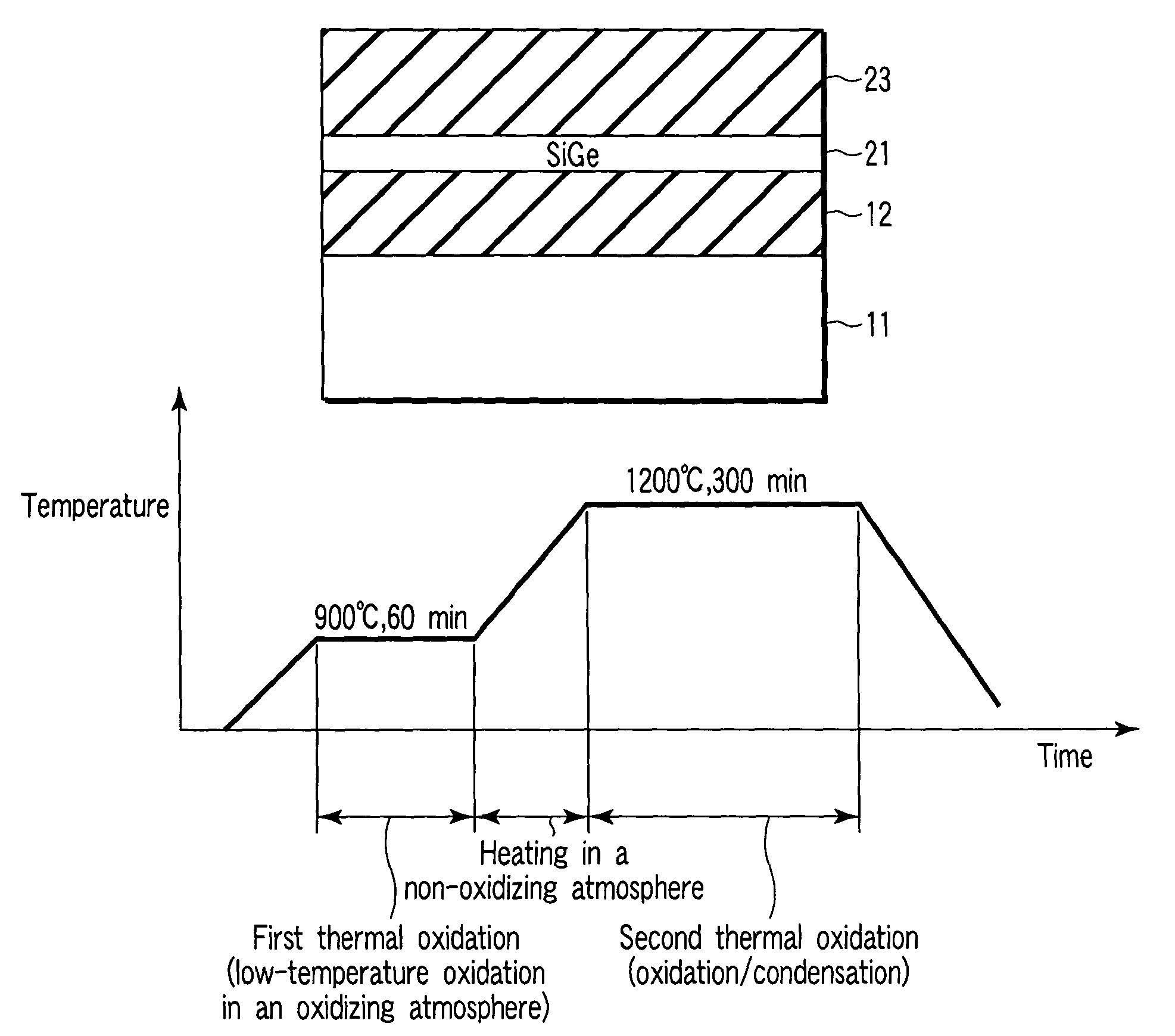
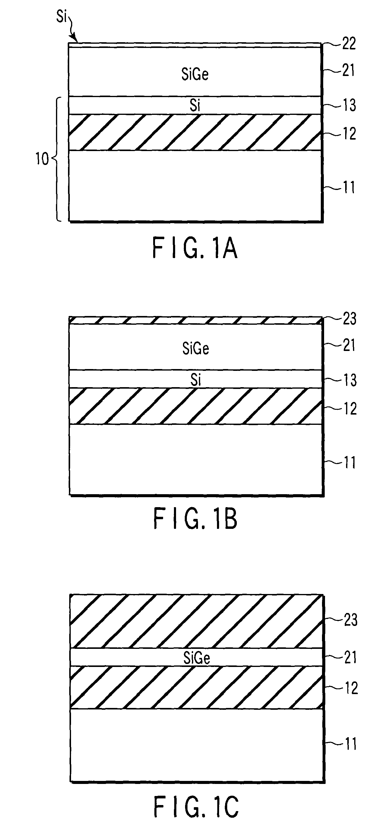
[0034]FIGS. 1A to 1C are sectional views showing the steps of manufacturing a semiconductor device according to a first embodiment of the invention.
[0035]First, an SOI substrate 10 is thereby prepared, which has, as shown in FIG. 1A, a Si (SOI) layer 13 having thickness of 50 nm is formed on a Si substrate 11 having plane orientation (100) through a buried oxide film 12. A thin film of SiGe alloy crystal is grow on the substrate 10, by using a vacuum CVD apparatus. The thin film is formed at substrate temperature of 600° C., with disilane partial pressure of 20 mPa and germane partial pressure of 30 mPa. A SiGe layer 21 having Ge composition of 10% and thickness of 180 nm is thereby formed.
[0036]The SiGe layer 21 remains in a strained state. After the SiGe layer 21 has been grown, the supply of germane gas is stopped. The growth of the Si layer is continued at the substrate temperature of 600° C. and the disilane partial pressure of 8 mPa. A Si cap layer (protective film) 22 having ...
second embodiment
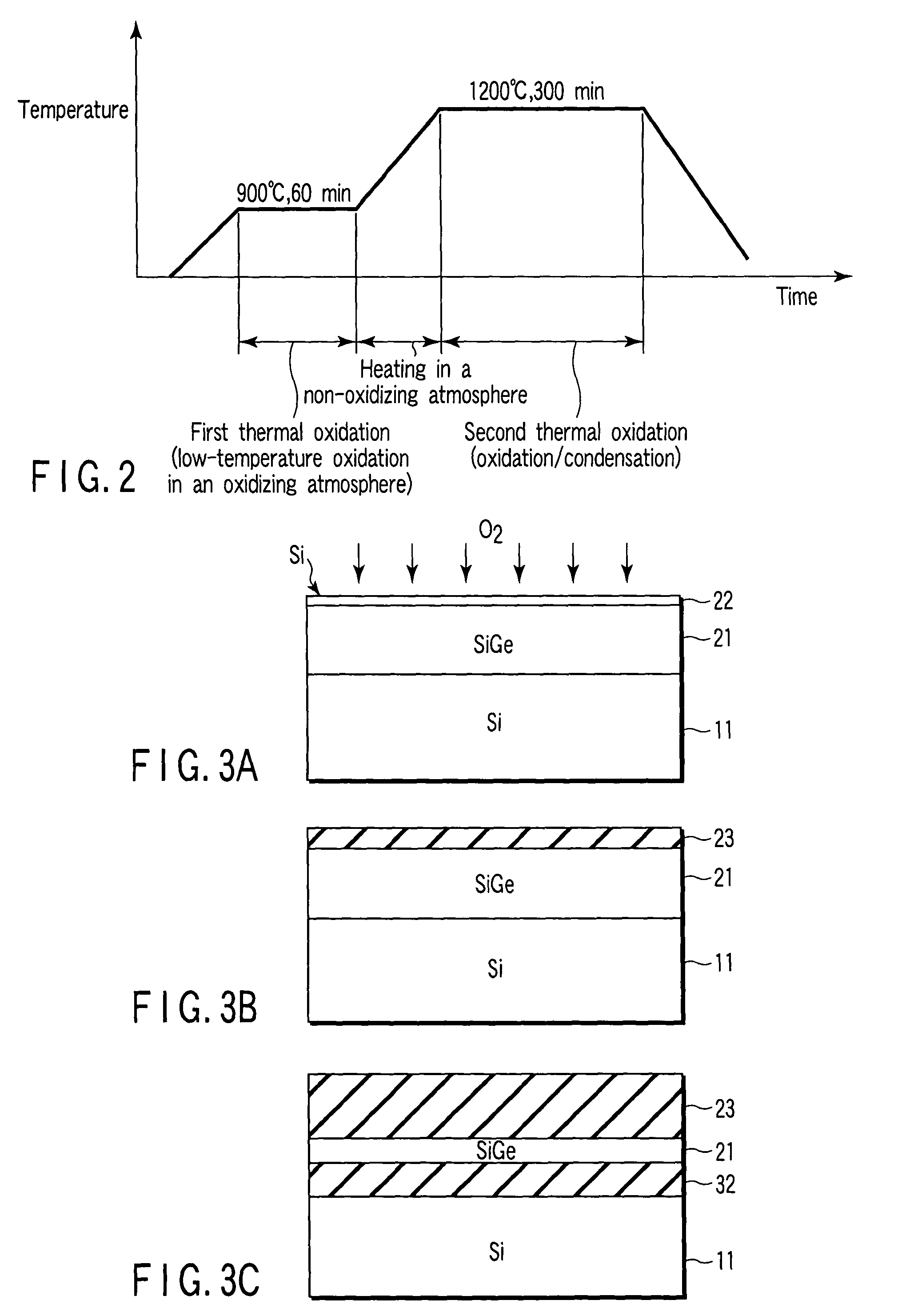
[0052]FIGS. 3A to 3C are sectional views showing the steps of manufacturing a semiconductor device according to a second embodiment of this invention. The components identical to those of the first embodiment are designated at the same reference numerals and will not be described in detail.
[0053]As described above, two oxidation steps are performed in the first embodiment. Two oxidation steps can be performed not only in an sample comprising a thin SOI substrate and a SiGe layer grown as crystal on the SOI substrate, but also applied to SIMOX processes. For example, a SiGe crystal layer (Ge composition of 10%) having thickness of 0.3 μm is formed on a Si substrate, and a Si cap layer (20 nm thick) is formed on the SiGe crystal layer. Oxygen ions are implanted into the substrate and the two oxidation steps are carried out. The SiGe crystal layer provided on the oxygen-added Si crystal layer therefore undergoes lattice relaxation. This achieves the same advantage as in the case where ...
third embodiment
[0060]In the first embodiment, a SiGe layer is formed on an SOI substrate having (100) plane, and a Si cap layer is formed on the SiGe layer, thereby forming an relaxed SGOI layer by means of oxidation and Ge condensation. In this step, the first oxidation that forms a protective film is performed at a low temperature of 1000° C. or less. This makes it possible to suppress the threading dislocations very much during the subsequent oxidation and Ge condensation (second thermal oxidation) that is carried out at high temperature. Hence, an SGOI substrate having a low density of dislocation can be provided.
[0061]If an SGOI substrate having low dislocation density is formed by using the oxidation and Ge condensation and further condensation is required for a higher Ge concentration, plane defects, i.e., slip planes that are (111) planes or similar planes, may develop. Some of these plane defects have misfit dislocation at the interface between the buried oxide film and the SGOI layer. Th...
PUM
| Property | Measurement | Unit |
|---|---|---|
| temperature | aaaaa | aaaaa |
| temperature | aaaaa | aaaaa |
| thick | aaaaa | aaaaa |
Abstract
Description
Claims
Application Information