Semiconductor device having high dielectric constant layers of different thicknesses

a technology of dielectric constant and semiconductor, applied in the details of semiconductor/solid-state devices, semiconductor devices, electrical apparatus, etc., can solve the problems of increased threshold voltage, difficult to induce enough carrier in the channel region, and inability to apply electric field to the gate, etc., to achieve the control of the threshold voltage of the p-type mosfet

Active Publication Date: 2010-07-20
RENESAS ELECTRONICS CORP
View PDF42 Cites 4 Cited by
  • Summary
  • Abstract
  • Description
  • Claims
  • Application Information

AI Technical Summary

Benefits of technology

[0015]The disclosure of C. Hobbs et al, entitled “Fermi Level Pinning at the Poly Si / Metal Oxide Interface”, 2003 Symposium on VLSI Technology Digest of Technical Papers describes that Fermi level pinning is caused when a high-k film such as HfO2 and the like is provided so as to contact with a polycrystalline silicon. Such Fermi level pinning is considerably influential to the operation of the P-type MOSFET. In particular, the influence to the P-type MOSFET becomes larger when the P-type MOSFET includes the high dielectric constant film containing Hf such as HfO2 and HfAlO. However, since the second high dielectric constant film in the P-type MOSFET is formed to have thinner film thickness in the present invention, the quantity of the metal, which is originally contained in the second high dielectric constant film and is diffused into the polycrystalline silicon film, is reduced, even though the second high dielectric constant film contacts with the polycrystalline silicon film, and thus the generation of the depletion layer in the polycrystalline silicon can be avoided. This can diminish the influence of Fermi level pinning to the P-type MOSFET. Therefore, the increase of the threshold voltage of the P-type MOSFET can be inhibited and the fluctuation thereof can also be reduced.
[0016]In addition, the high dielectric constant film in the N-type MOSFET can be formed to have larger film thickness, and thus the enhancement of the gate leakage current, which is a problem for the N-type MOSFET, can be also inhibited.
[0020]Diffusion, migration or the like of the metal contained in the first high dielectric constant film and the second high dielectric constant film into the semiconductor substrate can be prevented by providing the silicon oxide films between the semiconductor substrate and the first high dielectric constant film and between the semiconductor substrate and the second high dielectric constant film, respectively.
[0022]Fermi level pinning described above is considerably caused when the polycrystalline silicon film containing P-type impurity contacts with the high dielectric constant film. On the contrary, since the second high dielectric constant film in the P-type MOSFET is formed to have thinner film thickness in the present invention, the quantity of the metal, which is originally contained in the second high dielectric constant film and is diffused into the polycrystalline silicon film, is reduced, even though the second high dielectric constant film contacts with the polycrystalline silicon film, and thus the generation of the depletion layer in the polycrystalline silicon can be avoided.
[0024]The influence of Fermi level pinning can be moderated to reduce the threshold voltage and the increase of the gate leakage current can be inhibited by providing such relationship between the film thickness of the first high dielectric constant film and the film thickness of the second high dielectric constant film. When the first high dielectric constant film is composed of, for example, HfSiNO, the film thickness d1 may be equal to or higher than 1.5 nm. Having this configuration, the increase of the gate leakage current in the N-type MOSFET can be inhibited. In addition, the film thickness d2 of the second high dielectric constant film may be equal to or less than 1 nm, for example, and more preferably equal to or less than 0.5 nm. Having such configuration, the influence of Fermi level pinning can be reduced.
[0033]According to the present invention, the controllability of the threshold voltage of the P-type MOSFET within an desired range by reducing the threshold voltage of the P-type MOSFET is provided while preventing an increase of the gate leakage current in N-type MOSFET for the semiconductor device that comprises the N-type MOSFET and P-type MOSFET including high dielectric constant films.

Problems solved by technology

Sufficient electrical field cannot be applied to the gate insulating film due to an influence of such depletion layer even though a gate voltage is applied, and thus it is difficult to induce enough amount of carrier in the channel region.
As a result, a problem is arisen, in which a threshold voltage is increased, and further a fluctuation in the threshold voltage is also increased.
In such case, a problem is occurred that the gate leakage current generated in the N-type MOSFET is higher than that generated in the P-type MOSFET in the CMOS device.
On the other hand, a threshold voltage for the P-type MOSFET employing a high dielectric constant film containing a specific element such as Hf, Zr and the like is increased to a level that is higher than that for the P-type MOSFET employing silicon oxide for the gate insulating film, for the reason stated above, and is eventually increased to a level that provides a difficult situation in establishing a desired threshold voltage by adjusting density of an impurity in the Si substrate.

Method used


Image

  • Semiconductor device having high dielectric constant layers of different thicknesses
  • Semiconductor device having high dielectric constant layers of different thicknesses
  • Semiconductor device having high dielectric constant layers of different thicknesses

Examples


first embodiment

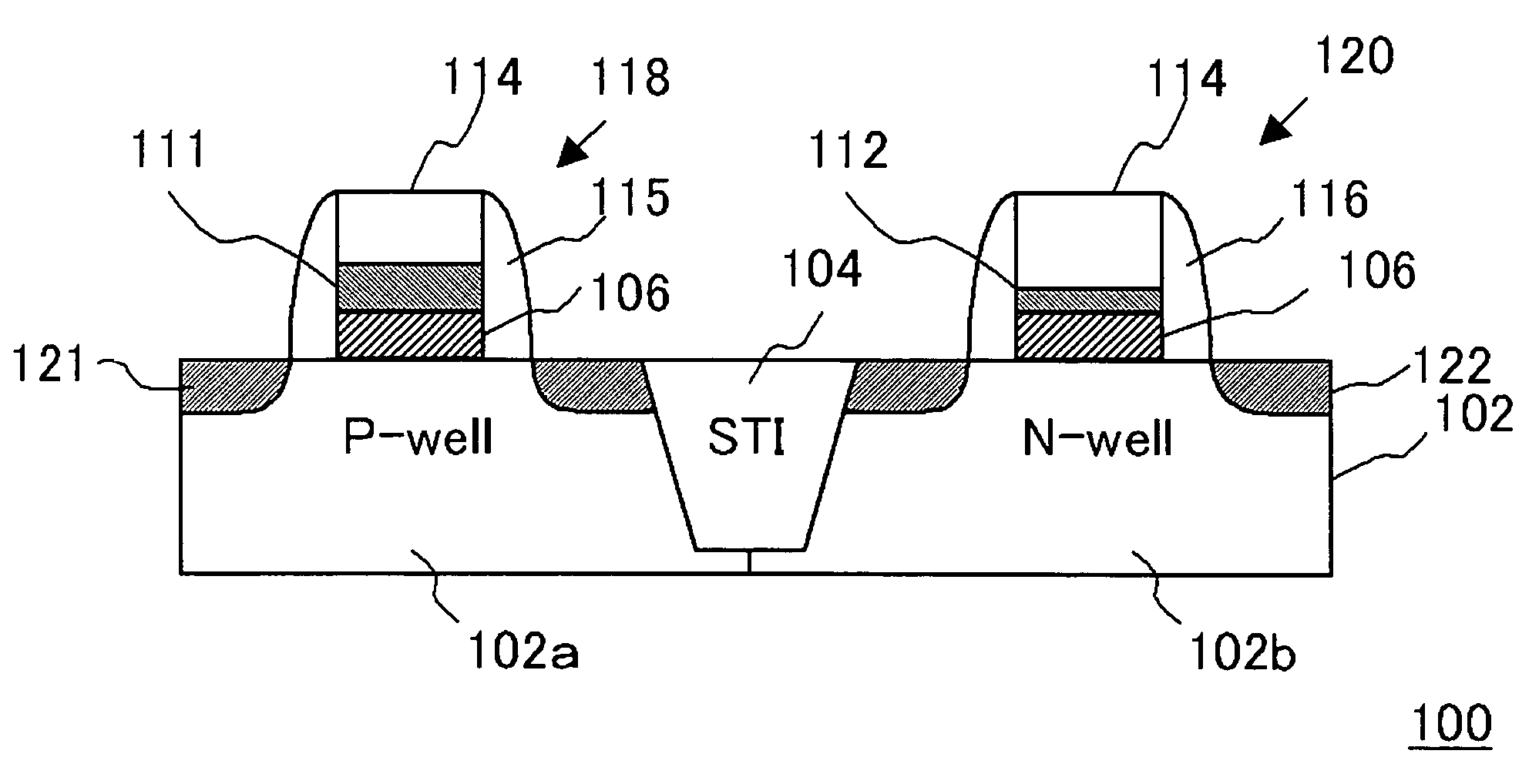
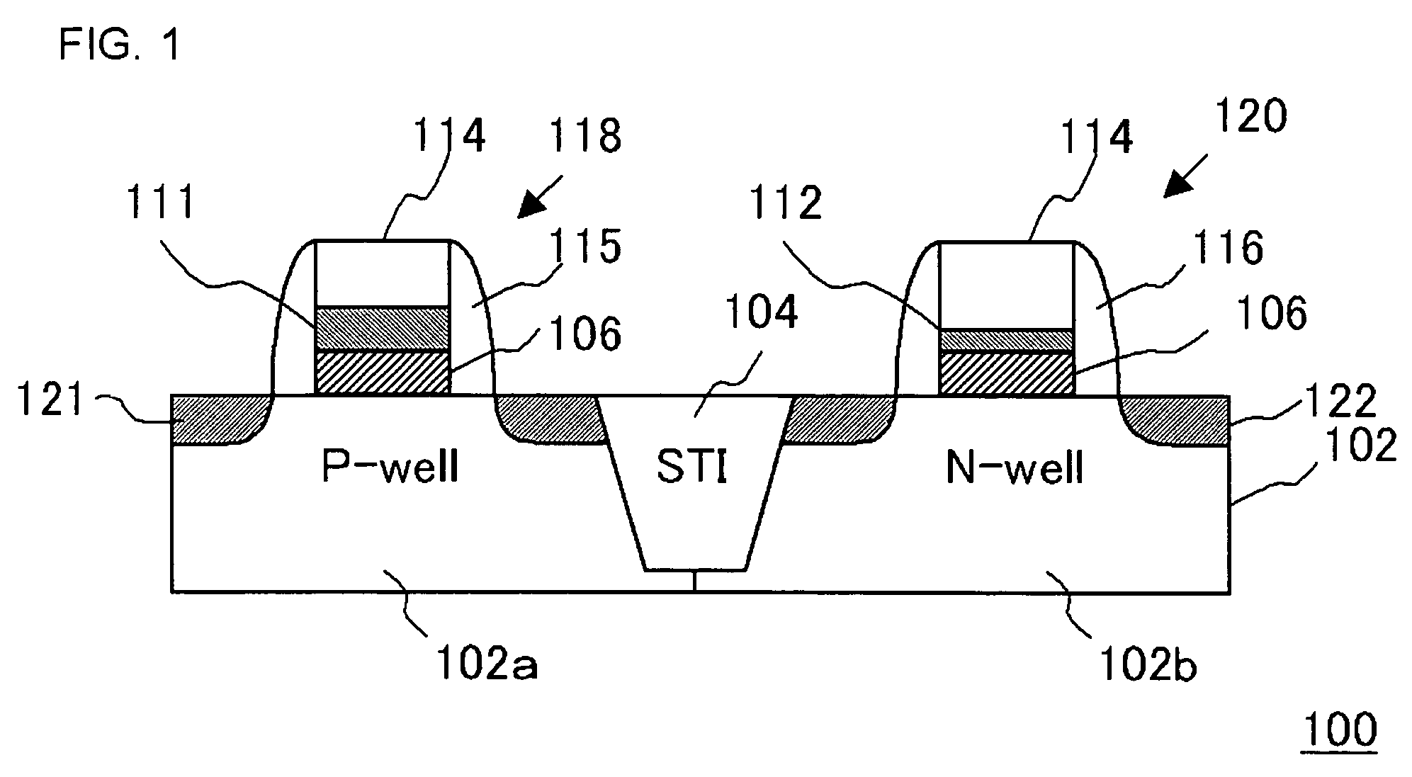
[0043]FIG. 1 is a cross-sectional view, illustrating a configuration of a semiconductor device in this embodiment.

[0044]In this embodiment, the semiconductor device 100 is a complementary metal oxide semiconductor (CMOS) device including an N-type MOSFET 118 and a P-type MOSFET 120. In addition, this CMOS device composes an internal circuit of a LSI.

[0045]The semiconductor device 100 comprises a silicon substrate 102, which has a P-well 102a of P-type conductivity and an N-well 102b of N-type conductivity provided thereon and a device separating-region 104 for separating the P-well 102a from the N-well 102b. An N-type MOSFET 118 and a P-type MOSFET 120 are formed in the P-well 102a and the N-well 102b, respectively.

[0046]A pair of impurity diffusion regions 121 is provided in the P-well 102a, and a channel region is formed therebetween. On the channel region is provided with a gate, which comprises a gate insulating film having a silicon oxide film 106 and a first high dielectric co...

second embodiment

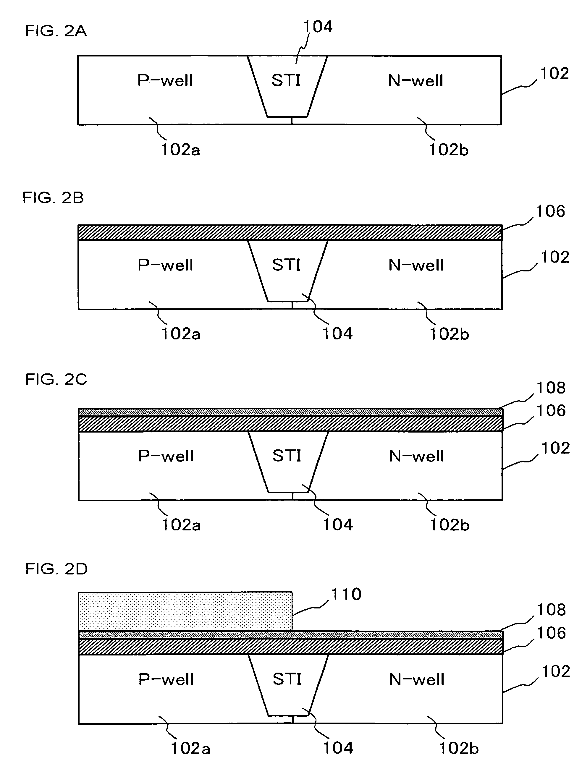
[0067]In this embodiment, similar process as described in the first embodiment in reference to FIG. 2A to FIG. 2D is conducted, and more specifically the silicon oxide film 106 and the high dielectric constant film 108 are formed on the silicon substrate 102 and the photo resist 110 is formed over the P-well 102a. A wet etching process is conducted by using, for example, diluted fluorinated acid (DHF) to selectively remove the high dielectric constant film 108 and the silicon oxide film 106 on the N-well 102b (FIG. 4). The present embodiment is different from the first embodiment in the point that the silicon oxide film 106 is also removed with the high dielectric constant film 108.

[0068]Subsequently, the photo resist 110 is removed and thereafter, a thermal oxidation is conducted on the surface of the N-well 102b of the silicon substrate 102 to form a silicon oxide film (not shown) on the N-well 102b. Subsequently, the high dielectric constant film is formed on the silicon oxide fi...

example

[0072]The P-type MOSFET 120 described in the first embodiment and having the configuration shown in FIG. 1 was employed to investigate a relationship of the film thickness of the second high dielectric constant film 112 with the threshold voltage in the P-type MOSFET 120. The results thereof are shown in FIG. 6.

[0073]As can be seen in the graph, thicker film thickness of the second high dielectric constant film 112 provides an increase of the threshold voltage in the P-type MOSFET 120. It was exhibited that the threshold voltage was in a level that is applicable to the manufacturing application (not higher than about 0.5 V) when the film thickness of the second high dielectric constant film 112 was equal to or less than 1 nm. In addition, it was found that the increase of the threshold voltage could be more effectively controlled by providing the film thickness of the second high dielectric constant film 112 as not greater than 0.5 nm. The P-type MOSFETs 120 having different film th...


PUM


Abstract

A semiconductor device 100 includes a silicon substrate 102, an N-type MOSFET 118 including a first high dielectric constant film 111 and a polycrystalline silicon film 114 on the silicon substrate 102, and a P-type MOSFET 120 including a second high dielectric constant film 12 and a polycrystalline silicon film 114 juxtaposed to N-type MOSFET 118 on the silicon substrate 102. The second high dielectric constant film 112 is formed to have the film thickness thinner than the film thickness of the first high dielectric constant film 111. The first high dielectric constant film 111 and the second high dielectric constant film 112 contains one or more element(s) selected from Hf and Zr.

Description

[0001]This application is based on Japanese patent application NO. 2004-144652, the content of which is incorporated hereinto by reference.BACKGROUND OF THE INVENTION[0002]1. Field of the Invention[0003]The present invention relates to a semiconductor device comprising an N-type metal oxide semiconductor field effect transistor (MOSFET) and a P-type MOSFET both containing high dielectric constant films.[0004]2. Description of the Related Art[0005]In recent years, the utilization of a thin film having high dielectric constant called high-k as a component material for semiconductor devices is actively investigated. Typical high-k materials include oxides of elements such as Zr, Hf and the like. The use of such materials for a gate insulating film of a MOSFET reduces a silicon oxide-conversion electrical thickness, even though the physical thickness of the gate insulating film is increased to a certain level, thereby providing physically and structurally stable gate insulating films. T...

Claims


Application Information

Patent Timeline
Patent Type & Authority Patents(United States)
IPC IPC(8): H01L29/76H01L31/119H01L31/113H01L31/062H01L29/94H01L27/01H01L27/12H01L31/0392H01L23/62H01L27/10H01L29/73H01L27/092H01L21/336H01L21/8238H01L29/78
CPCH01L21/823857H01L29/4916H01L29/513H01L29/517H01L2924/0002H01L2924/00
Inventor KIMIZUKA, NAOHIKOIMAI, KIYOTAKAMASUOKA, YURIIWAMOTO, TOSHIYUKISAITOH, MOTOFUMIWATANABE, HIROHITOTERAI, MASAYUKI
Owner RENESAS ELECTRONICS CORP
Why Eureka
Try Eureka