Photovoltaic devices with silicon dioxide encapsulation layer and method to make same

a technology of photovoltaic devices and silicon dioxide, which is applied in the direction of liquid/solution decomposition chemical coating, pv power plants, radiation control devices, etc., can solve the problems of inferior quality films and achieve the effect of high optical transparency

Inactive Publication Date: 2010-07-27
DE ROCHEMONT L PIERRE
View PDF20 Cites 42 Cited by
  • Summary
  • Abstract
  • Description
  • Claims
  • Application Information

AI Technical Summary

Problems solved by technology

Although this art instructs the use of liquid precursors comprising wet chemistry techniques that include carboxylic acid and alkloxide chemistries to form silicon dioxide and other oxide dielectrics, such as barium strontium titanate (BST), on integrated circuit substrates, the inventors repeatedly advise that heating the deposition chamber and substrate during the deposition process leads to inferior quality films.

Method used


Image

  • Photovoltaic devices with silicon dioxide encapsulation layer and method to make same
  • Photovoltaic devices with silicon dioxide encapsulation layer and method to make same
  • Photovoltaic devices with silicon dioxide encapsulation layer and method to make same

Examples


Embodiment Construction

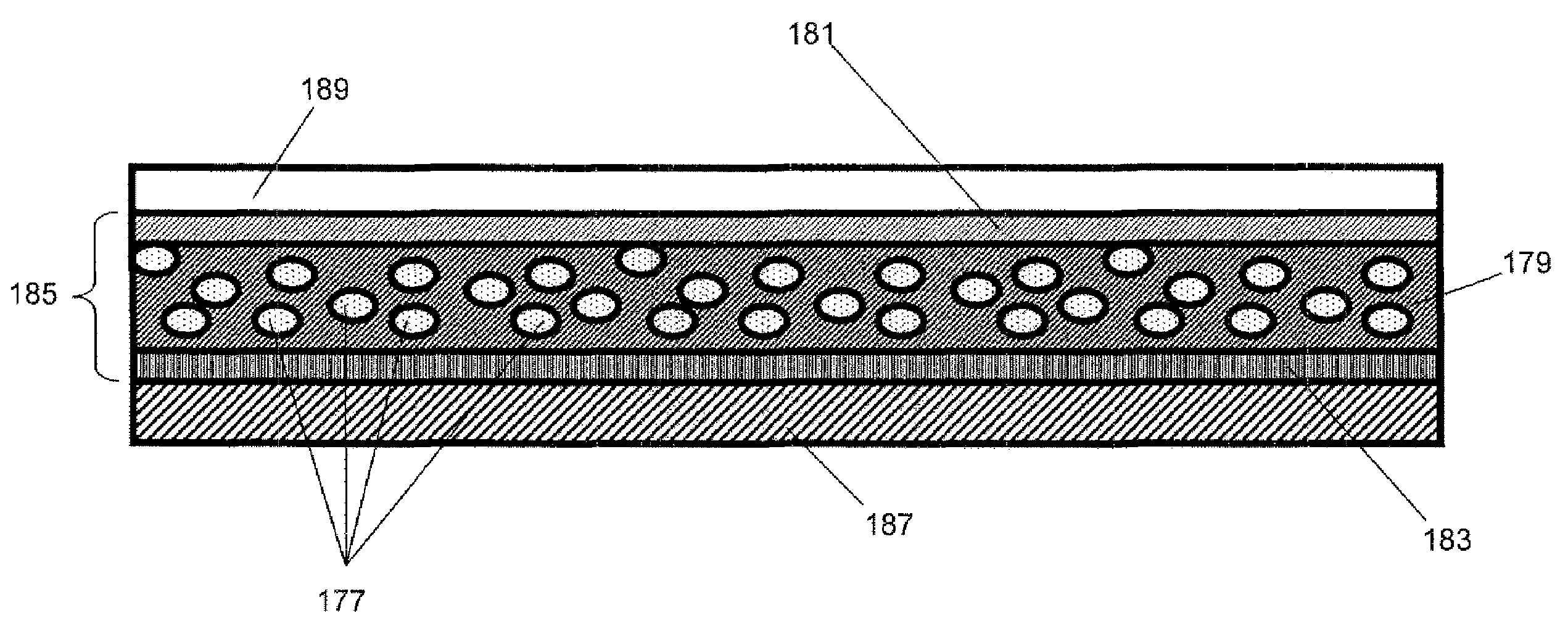
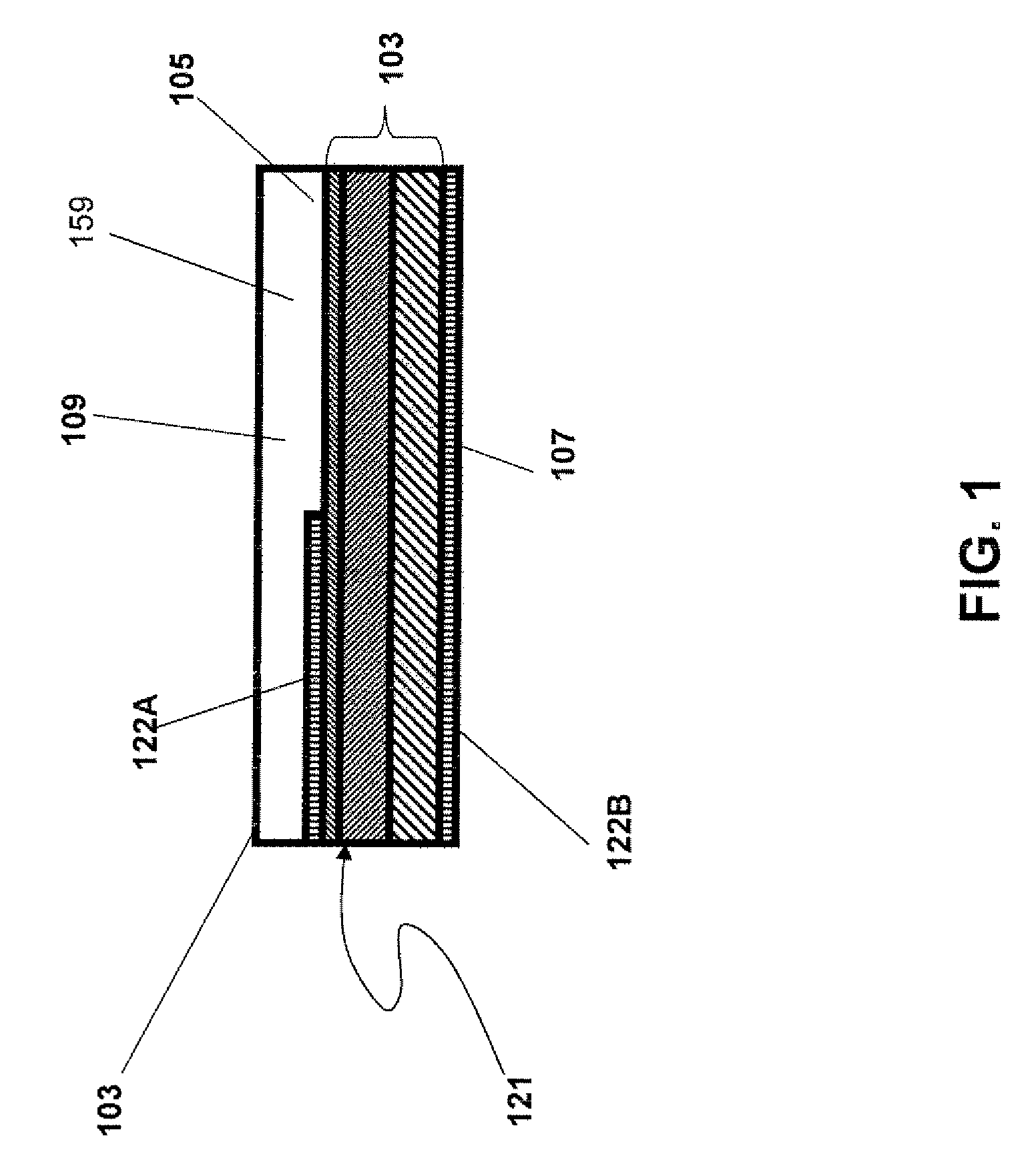
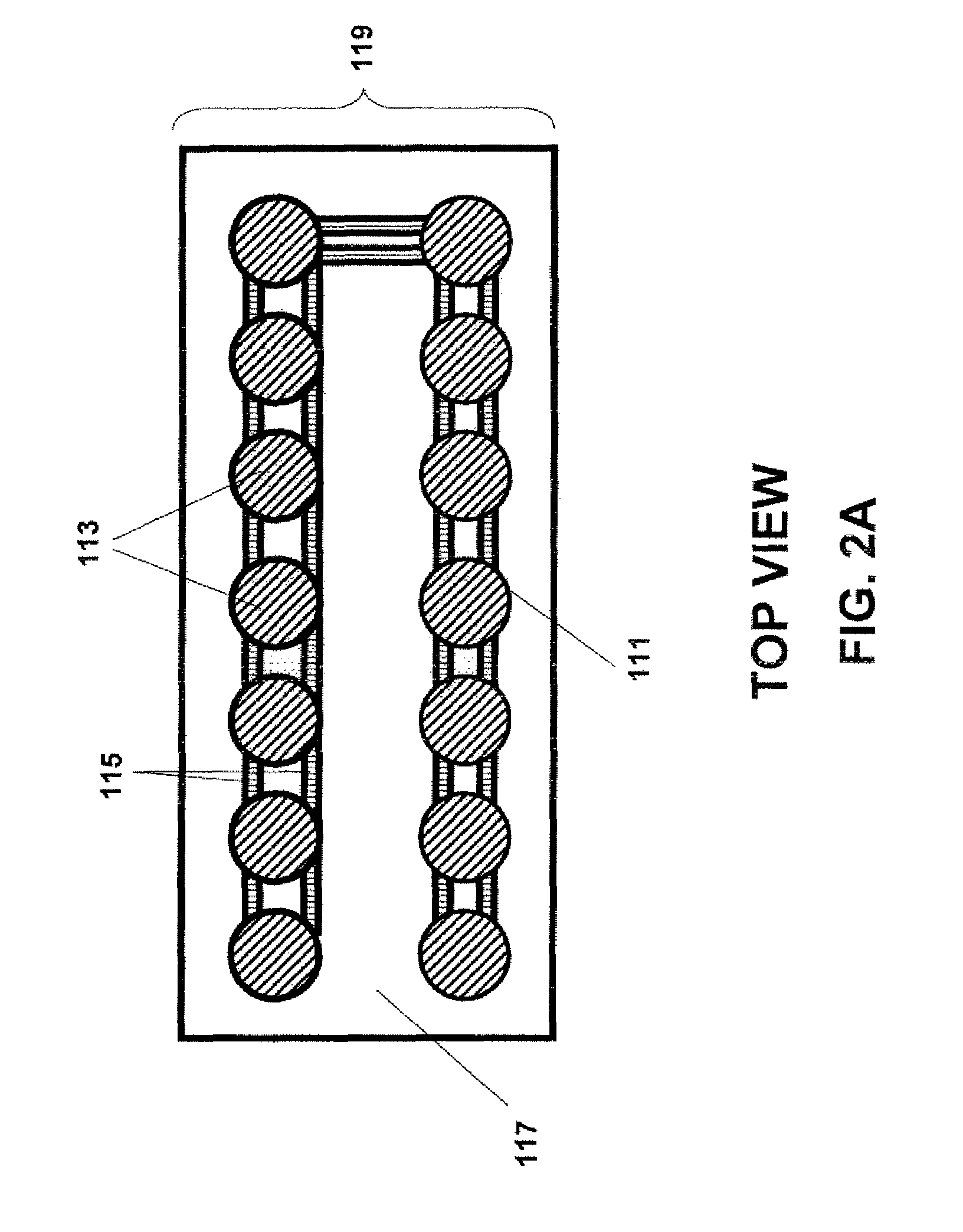
[0022]This application incorporates by reference all matter contained in co-pending U.S. patent application Ser. No. 11 / 243,422, filed Oct. 3, 2005 and entitled “CERAMIC ANTENNA MODULE AND METHODS OF MANUFACTURE THEREOF” (the '422 application), Ser. No. 11 / 479,159, filed Jun. 30, 2006 and entitled “ELECTRICAL COMPONENT AND METHOD OF MANUFACTURE” (the '159 application), and Ser. No. 11 / 620,042, filed Jan. 6, 2007 and entitled “POWER MANAGEMENT MODULES AND METHOD OF MANUFACTURE” (the '042 application). In the '422 application, de Rochemont, discloses articles and methods that are used to form silicon dioxide-based layers and meta-material bodies on the surface of a semiconductor die using low-temperature liquid or powder aerosol sprays.

[0023]Photovoltaic (PV) cells, more popularly known as solar cells, convert sunlight to direct current (DC) electrical energy that can be used to charge batteries, power a variety of microelectronic devices, or drive DC motors. PV systems can also be co...


PUM

PropertyMeasurementUnit
temperaturesaaaaaaaaaa
thicknessaaaaaaaaaa
temperaturesaaaaaaaaaa

Abstract

A photovoltaic device and method of manufacture provides a P-N junction formed between doped semiconductor materials and adapted to produce photovoltaic current in response to radiant energy reaching the P-N junction, and a silicon dioxide protective window layer located in proximity to doped semiconductor material and adapted to allow radiant energy to pass therethrough en route to the P-N junction, the protective layer including a high optical transparency layer of amorphous silica, having a silicon dioxide chemistry greater than 75 molar percent (75 mol %). A photovoltaic window provides a planar photovoltaic device being at least semi-transparent; and a pair of protective window layers sandwiched around the planar photovoltaic device and adapted to allow radiant energy to reach the photovoltaic device through both protective window layers, wherein at least one protective window layer is a high optical transparency layer of amorphous silica, having a silicon dioxide chemistry greater than 75 molar percent (75 mol %).

Description

RELATED APPLICATIONS[0001]The present application claims priority from U.S. Provisional Patent Application 60 / 761,725.FIELD OF THE INVENTION[0002]The present invention relates to photovoltaic devices having a high-transparency silicon dioxide environmental enclosure and the method to make the same.BACKGROUND[0003]U.S. Pat. No. 6,027,826 to de Rochemont, et al., disclose articles and methods to form oxide ceramic on metal substrates to form laminate, filament and wire metal-ceramic composite structures using liquid aerosol spray techniques. U.S. Pat. Nos. 6,323,549 and 6,742,249 to de Rochemont, et al., disclose articles that comprise, and methods to construct, an interconnect structure that electrically contacts a semiconductor chip to a larger system using at least one discrete wire that is embedded in silica ceramic, as well as methods to embed passive components within said interconnect structure. U.S. Pat. Nos. 5,707,715 and 6,143,432 to de Rochemont, et al., (the '715 and '432 ...

Claims


Application Information

Patent Timeline
Patent Type & Authority Patents(United States)
IPC IPC(8): H01L31/062H01L31/048
CPCC23C18/1212H01L31/02167H01L31/0384H01L31/04H01L31/048H01L31/18Y02E10/50H01L31/035218H01L31/1896
Inventor DE ROCHEMONT, L. PIERRE
Owner DE ROCHEMONT L PIERRE
Why Eureka
Try Eureka