Anti stark electrooptic medium and electrooptically modulated optoelectronic device based thereupon

a technology of optoelectronic devices and anti-smooth electrooptic mediums, which is applied in the field of ultra-high-speed optoelectronic devices, can solve the problems of increased absorption at the wavelength and bandgap shrinkage, and achieve the effect of increasing the overlap of electrons and strong increase of exciton oscillator strength

Active Publication Date: 2010-08-10
CONNECTOR OPTICS
View PDF13 Cites 14 Cited by
  • Summary
  • Abstract
  • Description
  • Claims
  • Application Information

AI Technical Summary

Benefits of technology

[0031]Semiconductor electrooptic medium is disclosed showing behavior different to a medium based on Quantum confined Stark Effect. A preferred embodiment of a new electrooptic medium comprises a type-II heterojunction, selected such, that, in zero electric field, an electron and a hole are localized on the opposite sides of the heterojunction having a negligible or very small overlap of the wave functions, and correspondingly, a negligible or a very small exciton oscillator strength. Applying an electric field results in squeezing of the wave functions to the heterojunction which strongly increases the overlap of the electron and the hole wave functions, resulting in a strong increase of the exciton oscillator strength.
[0032]Another embodiment of the new electrooptic medium includes a heterojunction between a layer and a superlattice, wherein an electron and a hole in the zero electric field are localized on the opposite sides of the heterojunction, the latter being effectively a type-II heterojunction. Yet another embodiment of the new electrooptic medium comprises a heterojunction between two superlattices, wherein an electron and a hole in a zero electric field are localized on the opposite sides of the heterojunction, the latter operating effectively as a type-II heterojunction. A further embodiment of the new electrooptic medium of the present invention comprises an ultrathin quantum well layer confined by barrier layers, having an essentially different barrier heights and a thick layer, wherein, in a zero electric field, a charged particle of one sign having a large effective mass is localized in this ultrathin layer, and a particle having a different sign of the charge, having a small effective mass is not localized in this ultrathin layer, but is localized mainly in the neighboring thick layer. Thus, the heterojunction between the two layers operates effectively as a type-II heterojunction. Applying an electric field to all types of the new electrooptic medium of the present invention results in a dramatic increase of the exciton oscillator strength and, therefore, in a large positive refractive index change at the photon energies below the exciton absorption peak. A very strong increase in the optical transition photon energy can be achieved, if necessary.
[0033]A strong electrooptic effect in a new electrooptic medium allows selecting modulator elements in optoelectronic devices having a larger thickness of the intrinsic conductivity layer, and thus, a lower capacitance, which, in turn, allows operation of the devices at higher frequencies. Shift of the exciton absorption peak to higher energies with bias makes the operation of the devices robust against temperature increase, which otherwise generally results (in conventional devices) in a bandgap shrinkage and leads in conventional Stark-effect devices to increased absorption at the wavelength of operation.
[0038]Another embodiment of the new electrooptic medium includes a heterojunction between a layer and a superlattice, wherein an electron and a hole in the zero electric field are localized on the opposite sides of the heterojunction, the latter being effectively a type-II heterojunction. Yet another embodiment of the new electrooptic medium comprises a heterojunction between two superlattices, wherein an electron and a hole in a zero electric field are localized on the opposite sides of the heterojunction, the latter operating effectively as a type-II heterojunction. A further embodiment of the new electrooptic medium of the present invention comprises an ultrathin quantum well layer confined by barrier layers, having an essentially different barrier heights and a thick layer, wherein, in a zero electric field, a charged particle of one sign having a large effective mass is localized in this ultrathin layer, and a particle having a different sign of the charge, having a small effective mass is not localized in this ultrathin layer, but is localized mainly in the neighboring thick layer. Thus, the heterojunction between the two layers operates effectively as a type-II heterojunction. Applying an electric field to all types of the new electrooptic medium of the present invention results in a dramatic increase of the exciton oscillator strength and, therefore, in a large positive refractive index change at the photon energies below the exciton absorption peak. A very strong increase in the optical transition photon energy can be achieved, when necessary.

Problems solved by technology

Shift of the exciton absorption peak to higher energies with bias makes the operation of the devices robust against temperature increase, which otherwise generally results (in conventional devices) in a bandgap shrinkage and leads in conventional Stark-effect devices to increased absorption at the wavelength of operation.

Method used


Image

  • Anti stark electrooptic medium and electrooptically modulated optoelectronic device based thereupon
  • Anti stark electrooptic medium and electrooptically modulated optoelectronic device based thereupon
  • Anti stark electrooptic medium and electrooptically modulated optoelectronic device based thereupon

Examples


Embodiment Construction

Electrooptic Medium Based on Anti-Stark Effect

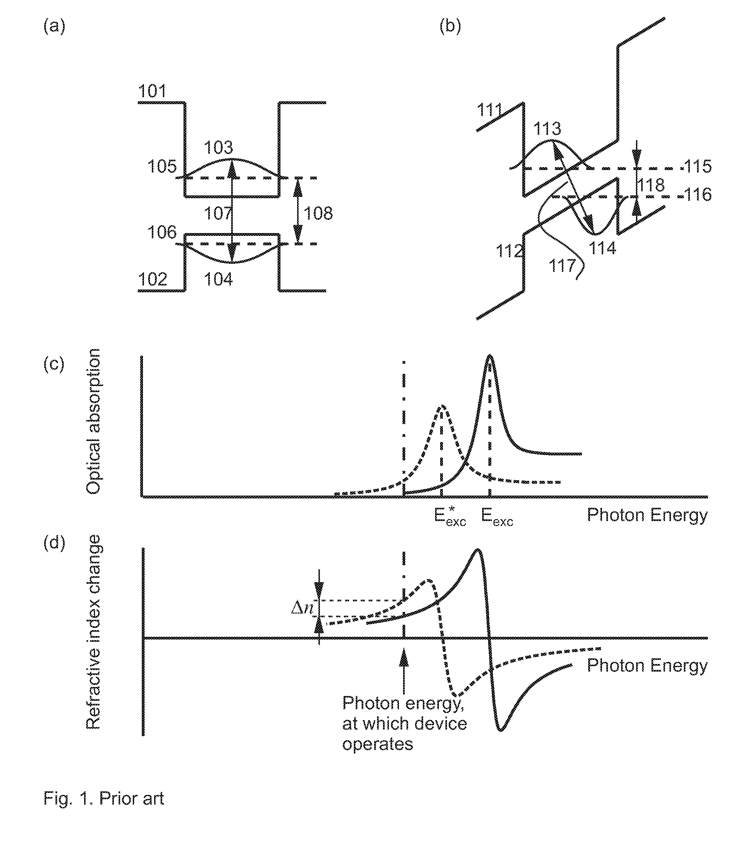
[0076]The present invention provides a novel electrooptic medium that allows to overcome major shortcomings of the conventional medium based on Quantum-confined Stark effect.

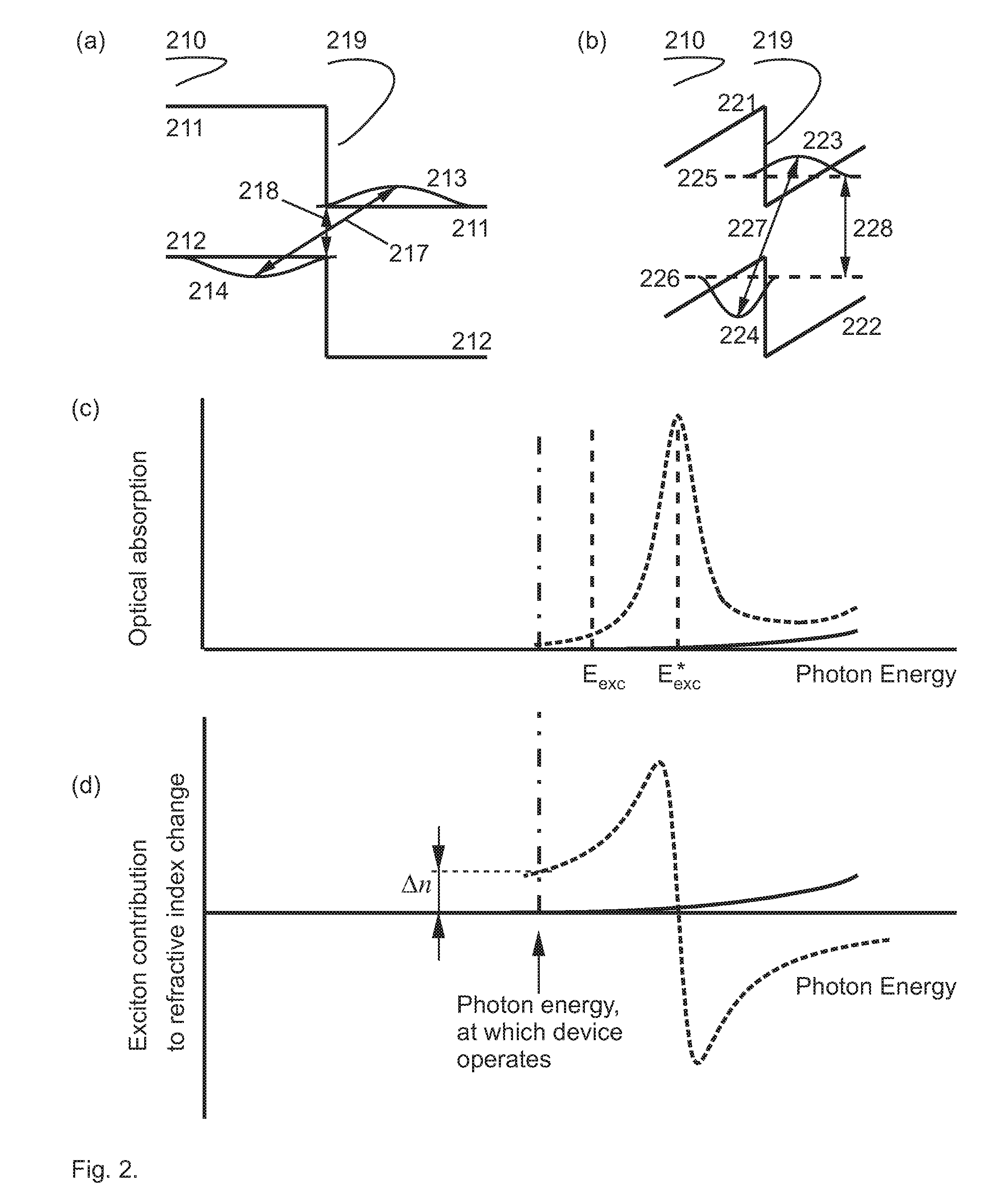
[0077]FIG. 2(a) shows schematically a type-II heterojunction (210), showing further the conduction band profile (211) and the valence band profile (212). The electron wave function (213) and the hole wave function (214) are confined separately on the opposite sides from the heterointerface (219). They are only weakly confined at the heterojunction due to the Coulomb interaction. The two wave function are spatially separated which illustrated by a diagonal line (217), and the overlap between the electron and hole wave functions is close to zero. Preferably the overlap between the electron wave function and the hole wave function defined by the overlap integral is below ten percent. The energy separation between two levels (218) is mainly determined by the separation b...


PUM


Abstract

Semiconductor electrooptic medium shows behavior different from a medium based on quantum confined Stark Effect. A preferred embodiment has a type-II heterojunction, selected such, that, in zero electric field, an electron and a hole are localized on the opposite sides of the heterojunction having a negligible or very small overlap of the wave functions, and correspondingly, a zero or a very small exciton oscillator strength. Applying an electric field results in squeezing of the wave functions to the heterojunction which strongly increases the overlap of the electron and the hole wave functions, resulting in a strong increase of the exciton oscillator strength. Another embodiment of the novel electrooptic medium includes a heterojunction between a layer and a superlattice, wherein an electron and a hole in the zero electric field are localized on the opposite sides of the heterojunction, the latter being effectively a type-II heterojunction. Yet another embodiment has a heterojunction between two superlattices, wherein an electron and a hole in a zero electric field are localized on the opposite sides of the heterojunction, the latter operating effectively as a type-II heterojunction.

Description

CROSS-REFERENCE TO RELATED APPLICATION[0001]This application claims the priority of provisional application 60 / 935,395, filed Aug. 10, 2007, entitled “Anti-Stark Electrooptic Medium and Electrooptically Modulated Optoelectronic Device Based Thereupon.” The priority benefit under 35 USC §119(e) of the provisional application is hereby claimed, and the application is incorporated herein by reference.BACKGROUND OF THE INVENTIONField of the Invention[0002]The invention pertains to the field of semiconductor devices. More particularly, the invention pertains to ultrahigh-speed optoelectronic devices, such as light-emitting diodes and laser diodes[0003]High-speed optoelectronic devices are broadly applied in modern data communication and telecommunication systems.[0004]These devices can be separated into two categories: those directly modulated by injection of current into the gain region, and those externally modulated. Direct modulation offers the advantage of low cost but requires very...

Claims


Application Information

Patent Timeline
Patent Type & Authority Patents(United States)
IPC IPC(8): H01L31/00H01S3/10
CPCB82Y20/00H01L31/0232H01L31/035236H04J14/02H01L31/147H01S5/0265H01L31/02325
Inventor LEDENTSOV, NIKOLAISHCHUKIN, VITALY
Owner CONNECTOR OPTICS
Why Eureka
Try Eureka