FIB based open via analysis and repair

a via analysis and open via technology, applied in the field of die level fault isolation yield improvement, can solve the problems of affecting the number and energy of secondary electrons emitted, one typical failure occurs, vias or contacts, etc., and achieve the effect of accurate detection of defects

Active Publication Date: 2010-08-31
DCG SYST
View PDF2 Cites 72 Cited by
  • Summary
  • Abstract
  • Description
  • Claims
  • Application Information

AI Technical Summary

Benefits of technology

[0020]It is therefore an object of this invention to provide a method for via / contact defect location and characterization which can more accurately locate defects, and in particular, resistive defects, opens, and shorts.

Problems solved by technology

One typical failure occurs when vias or contacts (i.e., vertical conducting connections) between metallization layers are either open or shorted laterally.
This results from differences in the charging of the feature in response to the beam, which affects the number and energy of secondary electrons emitted.
For all of the aforementioned reasons, use of an SEM does not provide as good a voltage contrast compared with the use of FIB.
This parallel processing is quite time consuming, since after etching each layer, the device must be returned to and viewed in an SEM to re-establish the “signal”, and then the parallel process / SEM cycle is repeated until the defect is found by VC, typically requiring several iterations.
Another weakness of the parallel process / SEM cycle is that the SEM can not identify issues in the next level, thus delayering may passes through the defect and detailed information of the defect is lost.
Identifying defects by PVC in test structures which are designed for that purpose can be relatively straightforward under the conditions outlined above, but identifying defects in actual circuits, for example for via chains which extend in z as described above, may be a more complex problem.
It may be necessary to use mechanical nano-probing to inject a voltage if for some reason the VC resolution is poor, possibly due to both ends of the node floating.
But the defect can be of many types: e.g., if the via hole was not completely etched, that is one issue; if the via hole has a void in the fill that is another issue; if the via hole was refilled during a photomask removal process, that is still another issue; if the via hole was never etched, that is another issue.
It is important to note that the cross sectioning process, either by FIB or by other means, is essentially destructive to the die, due to cutting and electrically isolating neighboring traces, as well as electrically shorting others during the trenching and polishing steps.
However, it is considerably less effective for locating resistive failures such as a high-resistance “open” via / contact.
A problem arising from the currently used failure analysis methods is that root cause diagnosis using cross-sectioning methods inherently destroys the structure or die.
This is a highly costly and time-consuming procedure.
Furthermore, if there are two defects in series, these techniques could generally not reveal them.

Method used


Image

  • FIB based open via analysis and repair
  • FIB based open via analysis and repair
  • FIB based open via analysis and repair

Examples


first embodiment

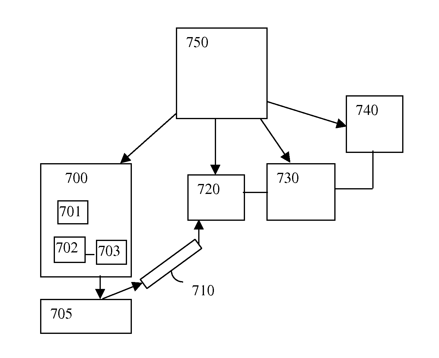
[0072]FIG. 6a summarizes a process flow of the present invention.

[0073]In step 600, deprocess sample globally to highest suspected level of defect, using FIB.

[0074]In step 605, contact two points on suspected net or sub-net with nanoprobes.

[0075]In step 610, apply dynamic voltage signal.

[0076]In step 615, check for defect on that level using DAVC.

[0077]In step 620, (optional), do capacitative and / or resistive analysis to locate and localize the defect.

[0078]In step 625, repeat steps 600-620 in a loop: continue deprocessing and checking for defect until defect level uncovered.

[0079]In step 630, use pseudo-cross sectioning to view and characterize defect (i.e., determine root cause) while removing it.

[0080]In step 635, use FIB to repair the defect.

[0081]In step 640 check to see that defect has been removed.

second embodiment

[0082]FIG. 6b illustrates a process flow of the present invention.

[0083]In step 645, deprocess the sample locally to the most accessible suspected defect net or sub-net.

[0084]In step 650, contact two points on the suspected net or sub-net with nanoprobes.

[0085]In step 655, do capacitive and / or resistive analysis to locate and localize the defect.

[0086]In step 660, repeat steps 645-655 until the defect level is uncovered and localized.

[0087]In step 665, use Pseudo-Cross Sectioning to view, characterize, and remove the defect.

[0088]In step 670, use FIB to repair the defect.

[0089]In step 675, check to see that the defect has been removed.

[0090]Comparisons to known good die or to simulated CAD / SPICE can be useful or even essential in either process flow. It is also possible to combine the above two embodiments. The process flow can move from that of FIG. 6a to that of FIG. 6b, although it is clumsy moving back and forth from the global deprocessing tools to the FIB. The flow can also mo...


PUM


Abstract

An improved method, apparatus, and control/guiding software for localizing, characterizing, and correcting defects in integrated circuits, particularly open or resistive contact/via defects and metal bridging defects, using FIB technology. An apparatus for identifying an abnormal discontinuity in a contact/via in an integrated circuit comprising a focused ion beam system to scan the ion beam over the contact/via to do remove or deposit via material, a detector to collect a secondary particle signal from the contact/via material that gets removed, a sub-system for storing the secondary particle signal from the contact/via in time as well as x-y scan position, a sub-system for correlating secondary particle signals and identifying discontinuities in the correlated secondary particle signals, a sub-system for optimizing the display of the abnormal discontinuity; and a computer to implement software aspects of the system.

Description

CROSS-REFERENCE TO RELATED APPLICATION[0001]This application is related to U.S. Provisional Application No. 60 / 876,790, filed Dec. 22, 2006, and claims priority therefrom.FIELD OF THE INVENTION[0002]This invention pertains to IC diagnostics and die level fault isolation yield improvement, and more specifically to finding failures in IC's and correcting them so that the fabrication process problems can be identified, design verification can proceed, or design-process interactions can be addressed.BACKGROUND OF THE INVENTION[0003]As integrated circuit dimensions continue to shrink, methods of failure analysis and debug must be continually refined, both for process and for design issues. One typical failure occurs when vias or contacts (i.e., vertical conducting connections) between metallization layers are either open or shorted laterally. Locating these defective vias / contacts and diagnosing the failure mechanism is crucial to addressing the problem, whether it be in the design or th...

Claims


Application Information

Patent Timeline
Patent Type & Authority Patents(United States)
IPC IPC(8): G01R31/304
CPCG01R31/2853G01R31/307H01L22/12
Inventor LUNDQUIST, THEODORE R.SHAH, KETANANAYAMA, TAMAYASUTHOMPSON, MARK A.
Owner DCG SYST
Why Eureka
Try Eureka